Large-format 2-layer FR4 boards with V-cut panelization and strict IPC-6011 Class 3 requirements often trigger detailed CAM engineering review. This case reviews a real production order (414 × 405.7 mm panel, 1.6 mm thick, 1oz copper) where multiple manufacturability conflicts emerged between the design intent and factory process capabilities. Issues centered on SMD-to-edge clearance, V-CUT alignment with legend, hole placement on outline, solder mask openings, and tight tolerances.
As a senior CAM engineer with over 15 years of experience, I frequently see how seemingly minor design details can lead to significant production risks on large panels. Our team raised several EQs to prevent edge defects, registration problems, and cosmetic failures that could compromise Class 3 reliability. This article walks through the actual issues discovered, the reasoning behind our recommendations, and the potential consequences if left unaddressed.
Order Overview
This was a 2-layer FR4 PCB ( #FR4-20260507-001 ) using TG150 material, 1.6 mm finished thickness, and 1oz copper on both sides. The board size was substantial at 414 × 405.7 mm, panelized 1×6 with V-cut plus routing. Surface finish was lead-free HASL, solder mask cold white on both sides, and black legend. Minimum hole size was 0.3 mm, with 100% flying probe testing required. Quantity was 180 pcs (30 sets). The customer specifically noted IPC-6011 Class 3 compliance as necessary. Mechanical forming and no resin plugging were specified.
The large panel size combined with V-cut depanelization and Class 3 demands created a narrower process window than standard boards. Such configurations commonly require careful review of outline-related features, edge clearances, and legend placement to maintain structural integrity and electrical reliability during and after production.
Main Engineering Questions Found During CAM Review
SMD Pads Too Close to Board Outline – Risk of Exposed Copper
We noticed multiple SMD pads positioned very close to the final outline. After reviewing the gerber and routing data, our CAM team identified that the clearance was insufficient for reliable solder mask dam and edge plating control on a V-cut panel. We raised this as a critical EQ because mechanical routing and V-scoring can cause slight edge chipping or mask pull-back.
Figure 1: SMD pads too close to board outline
If ignored, this would likely result in exposed copper along the board edges after depanelization. In a Class 3 product, exposed copper increases the risk of corrosion, short circuits during assembly, or contamination in humid environments. We have seen similar cases lead to assembly failures and scrap boards when edge defects violated IPC-A-600 acceptance criteria. Our engineer recommended confirming the minimum acceptable clearance or adjusting the pads to protect yield.
Legend Line Interference with V-CUT Path
A continuous line appeared in the middle of legend characters in the V-CUT area. We were uncertain whether this line indicated intended V-CUT processing or was part of the design graphics. Our production engineer flagged this because V-scoring must avoid damaging legend or underlying copper, especially on a large panel where registration tolerance is tighter.
Figure 2: a continuous line appeared in the V-CUT area
Proceeding without clarification could cause legend damage during scoring or misalignment that affects board separation. In the worst case, this leads to cosmetic defects or functional traces being compromised near the V-cut line, resulting in open circuits or yield loss. We asked the customer to confirm the intent so we could adjust the scoring depth and position accordingly.
2.0 mm NPTH Hole Located Directly on Outline
An arrow pointed to a 2.0 mm NPTH hole positioned exactly on the board outline. We needed confirmation whether this was intentional or a design oversight. Placing a hole on the outline during routing can cause breakout or incomplete hole formation on large panels.
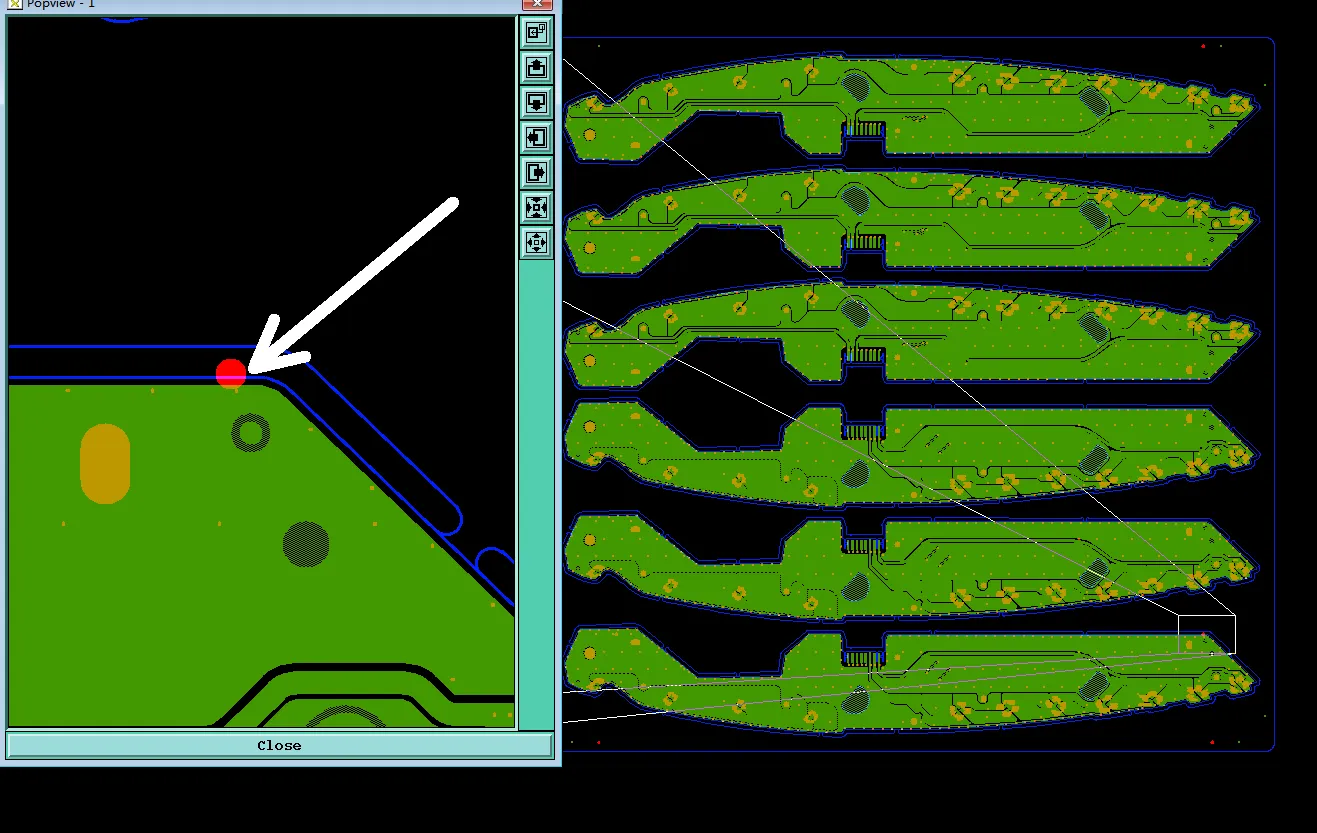
Figure 3: a 2.0 mm NPTH hole positioned exactly on the board outline
If not clarified, this configuration risks hole breakout, irregular edges, or mechanical weakness at the perimeter. For Class 3 boards, such defects often fail inspection and lead to scrap. Our team suggested verifying the hole intent and potentially moving it inward by a safe margin to maintain structural integrity.
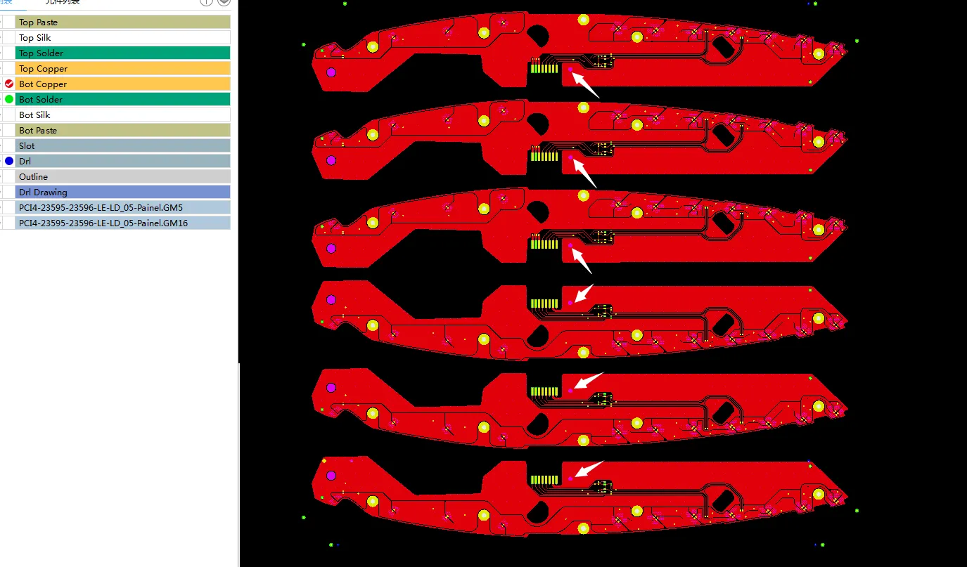
Gold Finger Bevel (Chamfer) Impossibility Due to Panelization Constraints
The customer data showed gold fingers, yet there was no explicit bevel requirement noted. During CAM review, we discovered that both sides of the fingers were blocked by routing slots narrower than 3 mm, making the standard beveling process mechanically impossible with our equipment. Our CAM engineer flagged this immediately because gold finger chamfering requires adequate clearance on both sides for the beveling tool to operate cleanly without damaging adjacent routing or features.
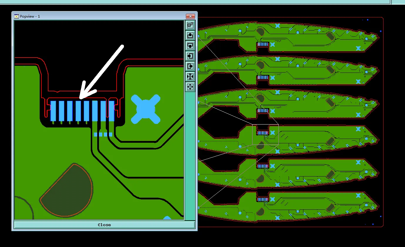
Figure 4: both sides of the fingers were blocked by routing slots narrower than 3 mm
If this had been ignored and we attempted beveling anyway, it could have resulted in tool interference, irregular edge damage, incomplete chamfer, or exposed copper on the finger edges. In IPC Class 3 applications, this often leads to poor connector mating, increased contact resistance, assembly failures, or long-term reliability issues in the field. We raised the EQ to confirm whether bevel was actually required. If not needed, we could proceed without it; if required, panel routing adjustments would be necessary to create sufficient clearance. This is a classic example of how panelization details can directly conflict with connector finishing requirements.
Solder Mask Opening Issue on 3.2 mm PTH Hole
On the bottom layer, a 3.2 mm PTH hole lacked the required solder mask opening. We identified that this would cause mask ink to flow into the hole during application. Our engineer recommended confirming whether the hole should remain open or if a specific mask clearance was intended.
Without adjustment, ink intrusion could block the hole, leading to poor plating contact, assembly issues with component pins, or unreliable through-hole connections. This is particularly problematic under flying probe testing and Class 3 reliability standards.
Legend Clarity and Tight Hole Tolerance
Characters with no gap between them would likely print blurry or merged. Additionally, the specified hole diameter tolerance was extremely tight and difficult to control consistently in production. These were noted as secondary but important for overall quality acceptance.
Manufacturing Risks and DFM Insights
Large panels with V-cut depanelization amplify the impact of insufficient edge clearances. Designers often overlook how routing and scoring tolerances interact with SMD pads and legend elements. On Class 3 boards, even minor edge copper exposure can fail long-term reliability testing due to potential dendritic growth or corrosion.
Tight hole tolerances on 1.6 mm boards with standard drilling processes are challenging to maintain across 180 pieces without statistical process control adjustments. If EQs are ignored, consequences include increased scrap rates, board warpage from unbalanced stress during V-scoring, assembly soldering defects, and multiple production review cycles that delay delivery.
This case reinforced the importance of clear fabrication notes separating design intent from manufacturing allowances, especially when IPC Class 3 is specified.
How the Engineering Team Resolved the Issues
We compiled detailed EQs with annotated screenshots showing problem areas and proposed solutions, such as adjusted clearances and mask openings. The customer confirmed the V-CUT path requirements, accepted minor legend adjustments, and clarified hole placements. Production numbering was added to the bottom legend layer as 2W7441279 with week/year code.
Our team then updated the CAM files, optimized the scoring program to avoid legend interference, and verified all edge features against IPC-6012 Class 3 criteria. These steps significantly reduced manufacturing risk before releasing the job to the shop floor.
Final Manufacturing Outcome
All engineering questions received customer confirmation. Manufacturing parameters were adjusted, files updated, and the order was approved for production. The panelization and outline-related issues were resolved within the standard process capabilities while maintaining the required Class 3 quality level.
Key Takeaways for PCB Designers
- Provide at least 0.3–0.5 mm clearance between SMD pads and final board outline, especially on V-cut panels, to prevent exposed copper after depanelization.
- Clearly indicate V-CUT paths in fabrication notes and avoid placing legend or critical features directly across scoring lines.
- Avoid placing holes exactly on the outline; include a small offset and specify NPTH/PTH intent explicitly.
- Define realistic hole diameter tolerances based on board thickness and quantity—consult manufacturer capabilities early for Class 3 jobs.
- Ensure solder mask openings are properly defined for all PTH holes to prevent ink intrusion.
- Use adequate spacing between legend characters and review data in a gerber viewer before submission.
- When specifying IPC Class 3, include detailed stackup and tolerance notes to reduce EQ volume.
- Coordinate panelization details with the fabricator if customer self-panelized to avoid registration surprises.
FAQ
Q1: Why is SMD pad to board edge clearance critical on V-cut panels?
A1: V-scoring and routing can cause slight edge material removal or mask retraction. Insufficient clearance often leads to exposed copper, increasing short circuit and corrosion risks, especially under IPC Class 3 standards.
Q2: What happens if a hole is placed directly on the board outline?
A2: It risks breakout, irregular hole shape, or incomplete formation during routing. This commonly causes mechanical weakness or inspection failures in production.
Q3: Why do CAM engineers pay close attention to legend over V-CUT areas?
A3: Scoring can damage or remove legend ink, affecting readability and potentially indicating deeper registration problems. Confirmation ensures proper scoring depth and position.
Q4: Can tight hole tolerances always be achieved on 2-layer boards?
A4: Not always, especially at higher quantities. Drilling process variation and material movement make ultra-tight tolerances difficult without special controls, often requiring customer discussion.
Q5: What is the risk of missing solder mask openings on PTH holes?
A5: Solder mask ink can enter the hole, blocking plating or component insertion. This leads to open circuits, poor solderability, or test failures during flying probe inspection.