










A 2-layer FR-4 panel measuring 520 mm × 242 mm arrived for CAM review as a customer-defined 1 × 3 array. The order specified TG150 material, 1.6 mm thickness, 1 oz copper on both sides, green solder mask, white silkscreen, leaded HASL, via tenting, V-cut separation, and zero process edge. Quantity was 60 pieces across 20 sets. Hole density reached 18 500 holes per square meter and minimum finished hole size was 0.3 mm. During data verification the panel connections, particularly a baffle feature at the lower-left corner, contained only solid copper-clad links with no stamp holes. Combined with the absence of process edge and reliance on V-cut, the structure presented a clear risk of board breakage during handling, plating, or shipping. The investigation centered on whether the panelization could survive manufacturing without additional break-away features.
Customer Panel Intent with Solid Connection Tabs
The board ( #FR4-20260429-023 ) designer intended a self-panelized array that would be separated by V-cut after delivery. The 1 × 3 layout occupied a large overall outline, and the internal connections between boards consisted of narrow solid tabs, including a baffle-like feature highlighted in the review. No stamp holes (mouse bites) had been placed on these tabs. Via tenting was specified, solder mask was supplied as a single layer, and certain holes showed asymmetric copper coverage. The overall goal appeared to be a cost-effective 2-layer panel that relied on the V-score lines alone for eventual separation. On a board of this size and hole density, however, the solid tabs become the primary structural elements that must keep the array intact through HASL, electrical test, and transport.
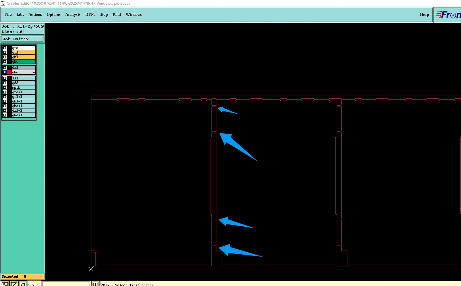
Figure 1: no stamp holes in the arrow indicated tab-routings
Solid Tabs and Zero Process Edge on Large V-Cut Array
Our CAM engineer examined the mechanical layer and the panel outline. The lower-left baffle and the intermediate connection tabs contained continuous copper and laminate with no perforations. Process edge was listed as zero, so no sacrificial margin existed outside the array. V-cut lines were present, yet the residual material between scores remained fully solid. On a 520 mm × 242 mm panel carrying high hole density, mechanical stress during racking, plating, and handling concentrates at these solid links. Without stamp holes the tabs must be broken by force after delivery; that force can initiate cracks that propagate into the functional board area.
If the solid tabs had been left unchanged, two realistic failure modes were expected. First, the panel could fracture spontaneously during HASL or flying-probe testing, producing scrap before the boards ever reached the customer. Second, even if the array survived shipping, the customer's depanelization step would require excessive force, risking edge cracks, copper lifting, or incomplete separation that violates IPC-A-600 edge-quality criteria. Either outcome would have compromised the 20-set order.
| Panel Feature | Observed Condition | Risk Without Stamp Holes | Recommended Addition |
|---|---|---|---|
| Lower-left baffle | Solid link, no perforations | High breakage probability under handling stress | Standard stamp-hole row |
| Intermediate tabs | Solid, no designed holes | Uneven force during depanelization | Stamp holes or confirm self-break |
| Process edge | Zero | No sacrificial margin | Rely on internal stamp holes |
Primary Conflict: Missing Stamp Holes on Critical Panel Links
The dominant conflict was a design-to-manufacturing mismatch between the supplied panelization geometry and the mechanical demands of a large, zero-edge, V-cut array. The customer data contained solid connection tabs and a baffle that provided no controlled break-away mechanism. Stamp holes are the conventional method of weakening such tabs so that the panel remains rigid through fabrication yet separates cleanly afterward. Their absence left the structural integrity of the array dependent on the tensile strength of continuous FR-4 and copper, which is insufficient for a 520 mm span under typical process loads.
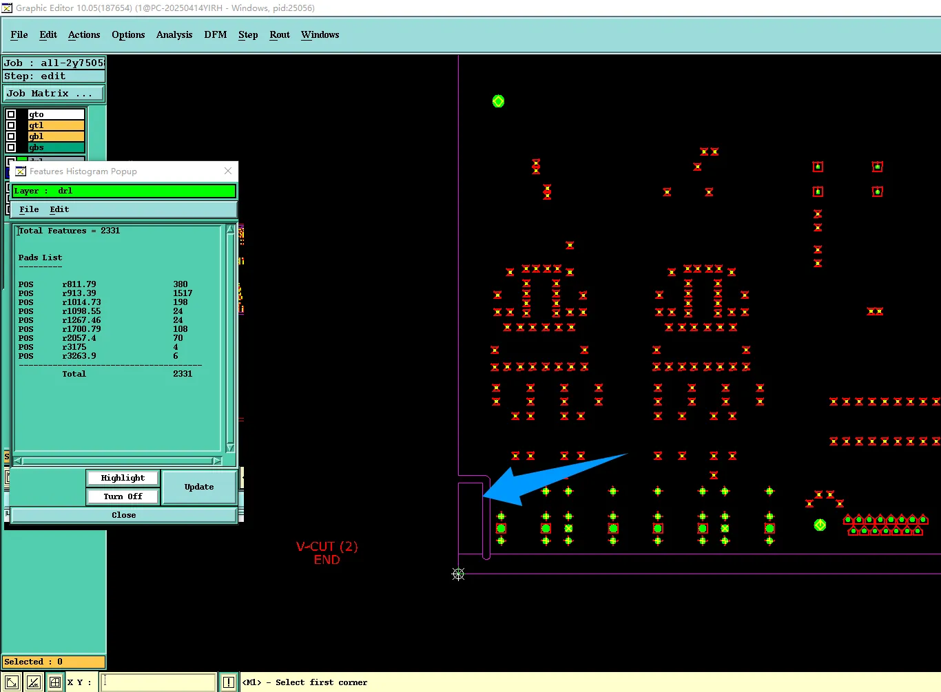
Figure 2: add tab routing at the lower-left corner of the indicated arrow area
Design intent could not be confirmed with certainty. It was possible the designer expected the customer to break the solid tabs by hand, yet the size of the panel and the zero process edge made uncontrolled fracture likely to damage the boards. It was equally possible that stamp holes had simply been omitted from the mechanical layer. Until the customer either authorized the addition of stamp holes or accepted responsibility for solid-tab breakage, the factory could not release a panel that carried a high probability of in-process scrap.
Supporting Observations on Mask and Hole Attributes
Secondary findings reinforced the need for a robust panel. Only one solder-mask layer had been supplied; the factory needed confirmation that the same openings applied to both top and bottom. Certain mask openings were larger than the finished hole yet smaller than the pad; these were candidates for deletion so that the holes could be treated as tented vias. Two drill locations showed copper on the bottom layer only, with no mask openings on either side, requiring attribute confirmation. English-language notes in the package were flagged for possible disregard. Each of these points required clarification, yet none altered the priority of the stamp-hole decision: a panel that breaks during processing renders mask and hole attributes irrelevant.
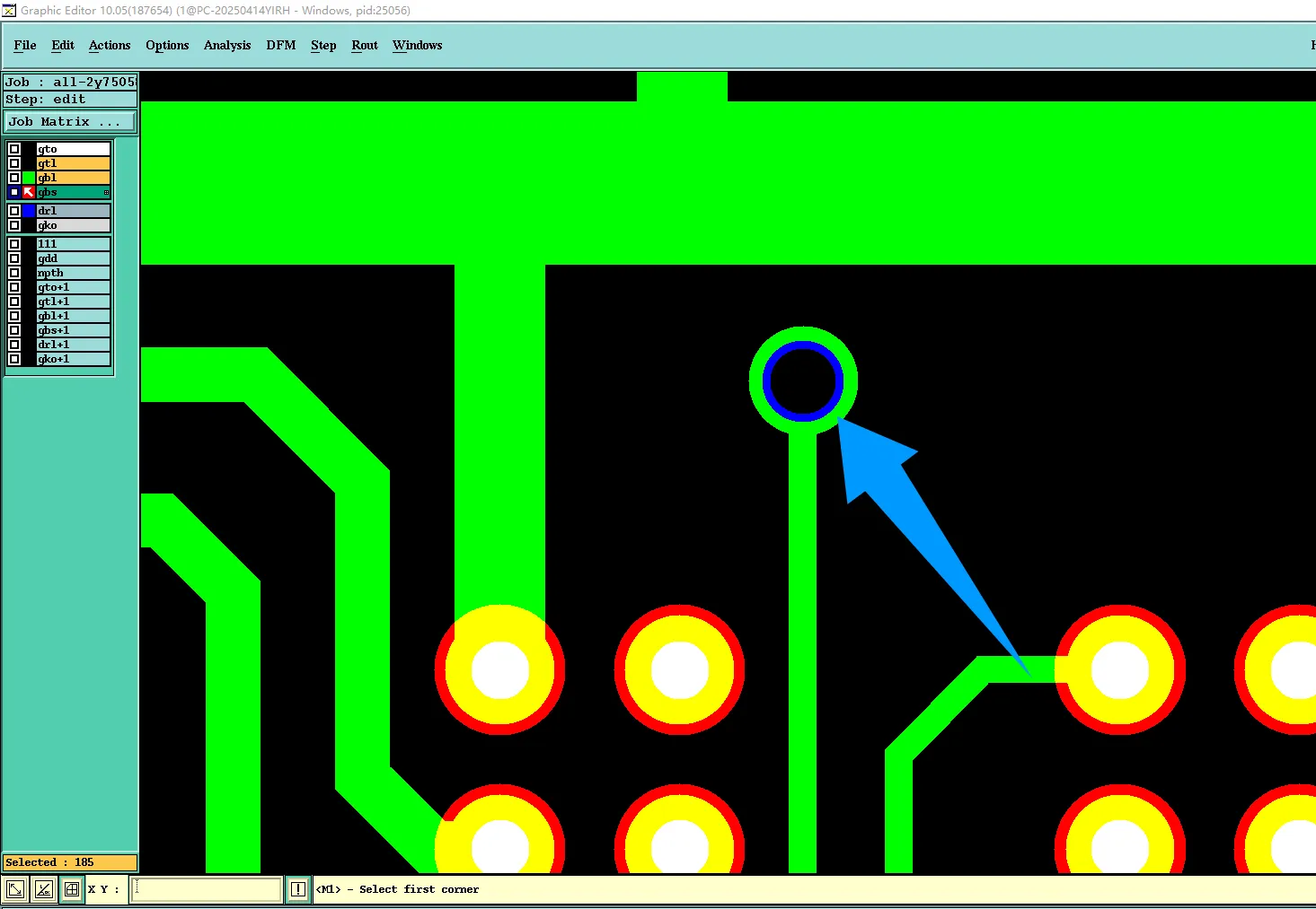
Figure 3: the opening is larger than the hole but smaller than the pad
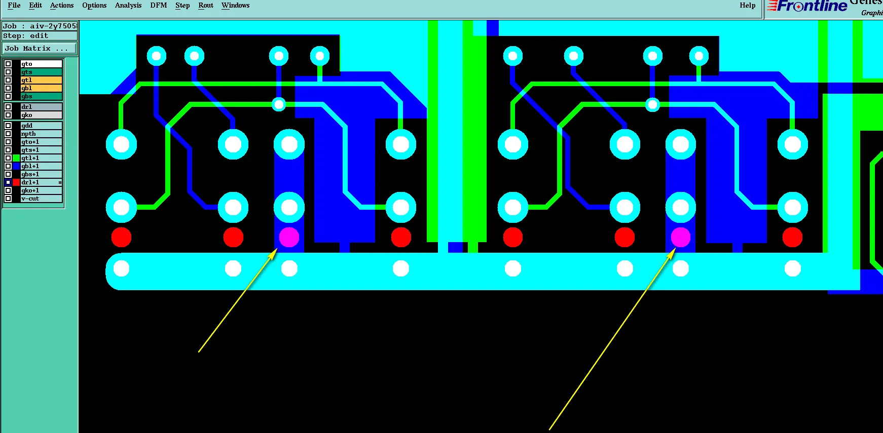
Figure 4: there is copper on the bottom layer, but no copper on the top layer
Stamp-Hole Addition and Final Panel Release
The engineering reply recommended adding a conventional row of stamp holes across the lower-left baffle and the intermediate solid links, following the factory's standard pitch and diameter for 1.6 mm FR-4 PCB. The addition would maintain panel rigidity through HASL and testing while allowing clean break-out at the customer site. Concurrently the single solder-mask layer would be applied to both sides, the oversized mask openings over vias would be deleted to achieve tenting, and the asymmetric copper holes would be attributed according to the customer's confirmation. English notes would be ignored as requested.
Customer acceptance authorized the stamp-hole addition and the accompanying mask and hole adjustments. The mechanical layer was updated, the panel data regenerated, and the job released for production. The 1 × 3 array retained its original outline while gaining the controlled break-away features required for reliable handling.
| Engineering Observation | Conflict Identified | Recommended Action | Final Status |
|---|---|---|---|
| Solid baffle and tabs, zero process edge | Breakage risk under process stress | Add stamp-hole rows | Implemented |
| Single solder-mask layer supplied | Top/bottom application unclear | Apply same openings to both sides | Confirmed |
| Mask openings larger than hole, smaller than pad | Unnecessary exposure | Delete openings, tent vias | Implemented |
| Asymmetric copper on two drills | Hole attribute undefined | Confirm plating status | Confirmed |
Design Lessons for Robust Stamp-Hole Panelization
- On any customer panel larger than approximately 300 mm with zero process edge, solid connection tabs should include stamp holes to prevent in-process breakage.
- V-cut alone does not replace the need for controlled break-away features when the residual tab width is narrow and the panel span is long.
- Stamp-hole diameter and pitch should follow the fabricator's standard for the board thickness so that the panel remains rigid through plating yet separates cleanly.
- When only one solder-mask layer is supplied, explicitly state whether the openings apply to both sides or provide separate top and bottom data.
- Mask openings that are larger than the finished hole yet smaller than the pad are usually deleted so the via can be tented; leaving them creates unnecessary copper exposure.
- Holes that show copper on only one side require an explicit plating attribute; silence forces an Engineering Question.
- High hole density increases panel stiffness variation; solid tabs on such boards are more prone to stress concentration and fracture.
FAQ
Q1: Why do missing stamp holes on a zero-edge V-cut panel create breakage risk?
A1: Solid tabs must absorb all handling and thermal stress. On a large panel the force required to break them later can crack the functional board area or cause spontaneous fracture during processing.
Q2: Can V-cut lines replace stamp holes for panel separation?
A2: No. V-cut weakens the score line but leaves the connection tabs fully solid. Stamp holes provide the controlled perforation needed for clean break-out.
Q3: What is the consequence of leaving solid tabs on a high-hole-density panel?
A3: The dense hole pattern creates local stiffness variations. Stress concentrates at the solid links, raising the probability of cracking during HASL or testing.
Q4: Why does a single supplied solder-mask layer require confirmation?
A4: The factory must know whether the openings apply to both top and bottom. Assuming symmetry without confirmation can produce incorrect mask coverage on one side.
Q5: When should mask openings larger than the hole but smaller than the pad be deleted?
A5: Such openings expose copper unnecessarily. Deleting them allows the via to be tented, protecting the hole and simplifying the mask process.
Q6: How should designers indicate hole attributes when copper is present on only one side?
A6: Explicitly mark the holes as plated or non-plated in the drill file or fabrication notes. Asymmetric copper without an attribute forces an Engineering Question.
```






