










PCB Specifications
| Parameter | Value | Parameter | Value |
|---|---|---|---|
| PCB Type | FR4 PCB | Quantity | 20 pcs |
| Layers | 2 Layers | Board Type | Panel PCB |
| Dimensions | 520 x 242 mm | Copper Weight | 1oz |
| Thickness | 1.6 mm | Min Track / Spacing | 6/6mil↑ |
| Surface Finish | HASL with Lead | Min Hole Size | 0.3mm↑ |
| Solder Mask | Green | Silkscreen | White |
| Stack-up | Custom | Impedance Control | No |
Manufacturing Timeline
Logistics Information
Key Manufacturing Processes
Manufacturing Summary
This 2-layer FR-4 board measured 520 × 242 mm with 1.6 mm thickness, TG150 material, and 1 oz copper on both sides. Produced as 60 pieces in 1×3 panels for 20 sets, the order used leaded HASL surface finish, green solder mask, and white silkscreen. Minimum holes were 0.3 mm with standard 6 mil line/space. V-cut separation was applied without process edges, and the 2-day schedule included 100% flying probe testing on the large-format panels.
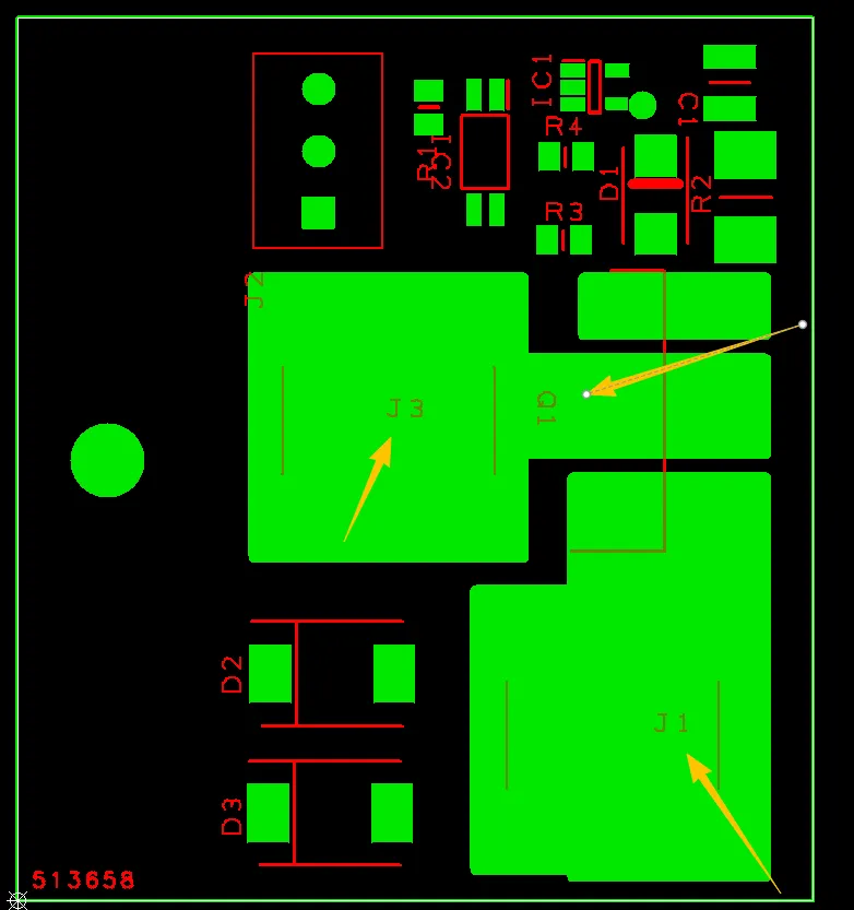
DFM review addressed panel integrity and mask consistency. English notes in the data were disregarded. A baffle region in the lower-left area lacked sufficient connection strength; a standard set of mouse bites was recommended to prevent breakage during handling. Only one solder-mask layer was supplied, so the same openings were applied to both top and bottom sides. Openings that were larger than the holes yet smaller than the pads were removed, and the corresponding holes were processed as tented vias. Small intermediate connection tabs contained no holes, raising the question of customer self-depanelization. Two drill locations showed copper on the bottom side only, with no top-side copper and no solder-mask openings, requiring confirmation of plated versus non-plated status.
Confirmed stamp-hole additions, mask-layer application, and hole-attribute decisions were implemented prior to production. The large boards achieved consistent HASL thickness consistency within the accelerated timeline. Full electrical test reports and quality certificates accompanied the shipment, confirming the panels met the specified mechanical and electrical requirements.
Explore More PCB Manufacturing Resources
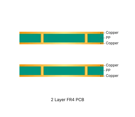
2 Layer FR4 PCB Manufacturing Insights
Discover how AIVON manufactures 2 Layer FR4 PCBs, including double-sided circuit structures, reliable through-hole fabrication processes, manufacturing challenges, and real production experience from customer orders.
Common Engineering Queries in 2 Layer FR4 PCB Design and Manufacturing
Real Engineering Queries (EQ) and DFM issues for 2 Layer FR4 PCB (double-sided boards) from actual production reviews. Learn how to avoid common problems with via treatment, silkscreen on pads, solder mask openings, hole attributes, board edge clearance, and other frequent design pitfalls.
Real Production Records
| Order ID | PCB Type | Layers | Dimensions | Solder Mask | Surface Finish | Quantity | Action |
|---|---|---|---|---|---|---|---|
| FR4-20260911-001 | FR4 PCB | 4 | 76.33 x 49.91 | Green | HASL Lead Free | 10 | View detail |
| FR4-20260910-004 | FR4 PCB | 2 | 69.92 x 69.91 | White | HASL Lead Free | 5 | View detail |
| FR4-20260907-001 | FR4 PCB | 2 | 90 x 40 | Green | HASL Lead Free | 30 | View detail |


