This 4-layer flexible circuit measured 86 mm × 46 mm with a finished thickness of 0.2 mm, rolled copper of 1/3 oz inner and 1/2 oz outer, yellow solder mask, white silkscreen, ENIG finish, laser outline, and a single 0.1 mm PI stiffener. The fabrication package also specified via tenting, 6 mil line and space, single-piece shipment, and flying-probe testing. During CAM review the combination of inconsistent mechanical-layer outlines, insufficient copper-to-edge clearance, and PI stiffener placement relative to the insertion fingers immediately raised process-capability questions. The central issue was whether the supplied FPC stiffener design rules and related geometric features could be manufactured repeatably without edge copper exposure, finger breakage, or dimensional instability under laser cutting and subsequent insertion forces.
The engineering assessment examined each observation against the physical limits of laser routing tolerance, stiffener adhesion, and thin-flex handling. Only after quantifying the capability margins was a revised manufacturing window established and released for production.
FPC Stiffener Outline Inconsistency Between GM and GM1 Layers
The Gerber mechanical layers presented two different outline definitions: the GM layer and the GM1 layer did not match in size. On a 0.2 mm flexible construction the final laser-cut contour is the sole reference for both electrical isolation and stiffener registration. When two competing outlines exist, the laser program cannot be generated without an arbitrary choice that risks either copper exposure or an undersized finished part.
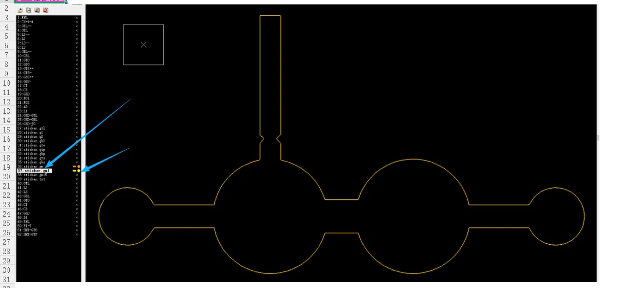
Figure 1: outlines on the GM layer and GM1 layer in the file are different
Process capability for laser routing of thin rolled-copper flex typically holds a positional tolerance of ±0.1 mm under controlled conditions. Selecting the incorrect outline therefore shifts the entire copper pattern relative to the finished edge by that amount. The engineering decision was to adopt the GM1 layer as the authoritative outline, document the selection, and obtain customer confirmation before any laser path generation. This single choice restored a unique geometric datum for all subsequent operations.
Copper-to-Outline Clearance and Laser Tolerance on 0.2 mm Flex
Both outer copper layers were drawn flush to the board ( #FPC-20260509-056 ) outline. Laser cutting of 0.2 mm polyimide-based material carries a process tolerance of 0.1 mm. When copper terminates at the nominal edge, the laser kerf and registration variation routinely leave partial gold-plated copper exposed at the perimeter. Exposed copper on an ENIG finish creates both a short-circuit risk to adjacent conductors or metal housings and a corrosion site under subsequent handling.
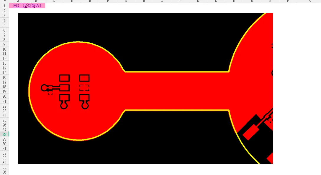
Figure 2: outer copper layers were drawn flush to the board outline
IPC-A-600 treats uncontrolled edge copper exposure as a workmanship defect once it extends beyond the intended land or mask boundary. The corrective action required a minimum 0.15 mm copper pull-back (inner cut) from the finished outline on both outer layers. This clearance absorbs the laser tolerance stack-up and leaves a dielectric margin that prevents gold exposure while remaining compatible with the 6 mil design rules. The pull-back was applied uniformly and submitted for confirmation.
| Feature | Customer Data | Process Capability | Engineering Assessment |
|---|---|---|---|
| Copper-to-outline spacing | 0 mm (flush) | ≥0.15 mm after laser | Exposure risk if unchanged |
| Laser outline tolerance | Not stated | ±0.1 mm typical | Must be absorbed by pull-back |
| Finished thickness | 0.2 mm | 0.2 mm nominal | Amplifies edge sensitivity |
PI Stiffener Placement Relative to Insertion Fingers
While the contract specified a single 0.1 mm PI stiffener for the insertion-finger region, a critical DFM issue was identified regarding the distance of the PI stiffener from FPC gold finger opening. In the original design, the stiffener edge terminated too close to the finger roots, creating a sharp bending moment during repeated ZIF connector insertion. To prevent polyimide fatigue cracking and eventual fracture at the stiffener transition, it is essential to maintain a clearance of at least 0.5 mm from the finger base.
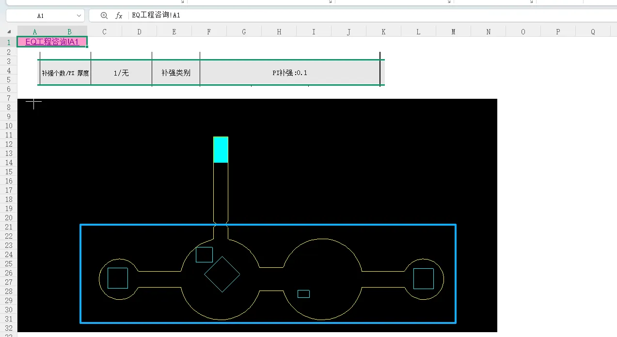
Figure 3: only one stiffener and located in the finger area
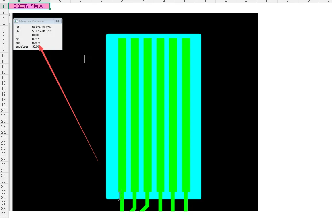
Figure 4: the stiffener edge terminated too close to the finger roots
Process experience with 0.1 mm PI stiffeners on 0.2 mm flex shows that a minimum 0.5 mm overlap beyond the finger root distributes the bending stress and significantly raises the insertion-cycle life. The engineering recommendation was therefore twofold: (1) restrict stiffener application to the finger region only, discarding extraneous GM15 geometry, and (2) enlarge the stiffener outline so that its edge remains at least 0.5 mm from the finger roots. Both changes restore a controllable mechanical transition while preserving the original reinforcement intent.
| Stiffener Parameter | Supplied Condition | Recommended Window | Risk if Unchanged |
|---|---|---|---|
| Application area | Multiple regions in GM15 | Finger region only | Unnecessary stiffness elsewhere |
| Edge-to-finger clearance | Insufficient | ≥0.5 mm | Finger breakage under insertion |
| Thickness | 0.1 mm PI | 0.1 mm PI | Within capability |
Via Geometry Anomalies Crossing Circuit Layers
Two vias in the supplied data extended onto the circuit layers in a manner inconsistent with normal plated-through construction. On a 0.2 mm four-layer flex the via aspect ratio is already low; any unintended copper connection between layers can create short circuits or alter the intended netlist. The observation was flagged for customer confirmation of data integrity. Once confirmed as an artwork error, the vias were corrected to standard plated-through geometry before drilling and plating.
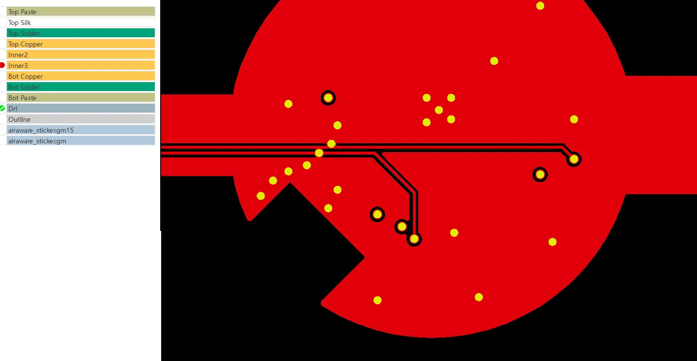
Figure 5: two vias in your files that extend into the trace layer
Physical Process Windows for Laser Routing and Stiffener Bonding
Laser routing of 0.2 mm rolled-copper flex operates inside a narrow geometric window. The combination of beam kerf, material shrinkage after coverlay cure, and registration between copper and mechanical layers must remain inside ±0.1 mm. When copper is drawn flush to the outline, that window collapses and gold exposure becomes statistically inevitable. The 0.15 mm pull-back re-opens the window and brings the process back inside demonstrated capability.
PI stiffener bonding adds a second constraint. The adhesive system requires a minimum overlap length to develop full peel strength; at the same time the stiffener edge must sit far enough from the flexing zone to avoid a stress concentration. A 0.5 mm clearance satisfies both adhesion and fatigue requirements for 0.1 mm PI on 0.2 mm flex. Restricting the stiffener to the finger region only further prevents unintended local stiffening that would otherwise transfer stress into adjacent copper features.
The integrated process sequence that satisfied all limits was:
- Adoption of GM1 as the sole outline datum
- Uniform 0.15 mm copper pull-back on outer layers
- Restriction of 0.1 mm PI stiffener to the insertion-finger zone
- Enlargement of stiffener outline to maintain ≥0.5 mm clearance from finger roots
- Correction of anomalous via geometry
- Standard laser routing, ENIG, and flying-probe verification
Each step was verified against existing process-capability data for laser positional accuracy, stiffener peel strength, and edge-copper integrity before the revised package was released.
| Process Element | Original Condition | Adjusted Condition | Capability Status |
|---|---|---|---|
| Outline datum | GM ≠ GM1 | GM1 selected | Unique reference restored |
| Copper-to-edge | 0 mm | 0.15 mm pull-back | Exposure eliminated |
| Stiffener-to-finger | Insufficient | ≥0.5 mm | Breakage risk reduced |
| Stiffener extent | Multiple regions | Finger zone only | Intent preserved |
Capability Verification by Dimensional and Mechanical Checks
Prototype panels incorporating the GM1 outline, 0.15 mm copper pull-back, enlarged finger-region stiffener, and corrected vias were processed through the standard laser, plating, and bonding sequence. Optical measurement confirmed that the finished copper edge remained ≥0.15 mm inside the laser contour on both sides. Stiffener placement verification showed a consistent ≥0.5 mm clearance from the finger roots and complete absence of extraneous stiffener areas. Peel testing of the 0.1 mm PI stiffener met the minimum adhesion values established for production lots. Flying-probe continuity verified that the corrected vias produced no unintended shorts. These results established that the revised data package operated inside a stable manufacturing window.
Approved Manufacturing Window and Release Decision
The final disposition retained the original 0.2 mm four-layer rolled-copper construction, yellow solder mask, ENIG finish, and 0.1 mm PI stiffener while implementing four controlled adjustments: (1) exclusive use of the GM1 outline, (2) 0.15 mm copper pull-back from the finished edge, (3) restriction and enlargement of the stiffener to maintain ≥0.5 mm clearance at the insertion fingers, and (4) correction of the anomalous via geometry. These changes restored usable process margins for laser positional accuracy, edge-copper integrity, and insertion durability without altering the functional circuit pattern.
The case illustrates that flexible PCB design rules are not merely geometric preferences; they define the boundary between a flex circuit that survives repeated insertion and one that fractures at the stiffener transition. By quantifying the capability margins for outline selection, copper pull-back, and stiffener-to-finger clearance, the engineering team converted an otherwise marginal data package into a production-ready construction.
FAQ
Q1: Why must copper features on laser-cut FPC maintain a minimum pull-back from the outline?
A1: Laser routing of 0.2 mm flex carries a typical tolerance of ±0.1 mm. When copper is drawn flush to the nominal edge, the kerf and registration variation leave gold-plated copper exposed. A 0.15 mm pull-back absorbs the tolerance stack-up and prevents both short-circuit and corrosion risks.
Q2: How close can a PI stiffener terminate relative to insertion fingers?
A2: Process data for 0.1 mm PI on 0.2 mm flex show that a clearance of less than approximately 0.5 mm creates a sharp stress concentration during ZIF insertion. Maintaining ≥0.5 mm distributes the bending moment and raises the number of insertion cycles before fatigue cracking appears.
Q3: Why is a single authoritative outline layer required when multiple mechanical layers exist?
A3: Laser path generation can reference only one contour. When GM and GM1 differ, the finished part will be either oversized or undersized relative to the copper pattern. Selecting one layer (in this case GM1) restores a unique geometric datum and eliminates ambiguity in registration.
Q4: What risk arises when a stiffener layer contains geometry outside the intended reinforcement zone?
A4: Extraneous stiffener areas locally increase flexural rigidity. During handling or insertion the stress is transferred into adjacent unsupported copper, raising the probability of trace cracking. Restricting the stiffener to the finger region only preserves the original mechanical intent without introducing secondary failure modes.
Q5: How does rolled copper thickness influence edge-exposure sensitivity on thin FPC?
A5: Thinner outer copper (1/2 oz) etches and plates more rapidly, but the absolute edge location remains governed by the laser tolerance. The same 0.15 mm pull-back is required regardless of copper weight once the finished thickness drops to 0.2 mm, because the dielectric margin is the controlling factor.
Q6: Why must anomalous via geometry be confirmed before plating on a four-layer flex?
A6: On a 0.2 mm stack-up any unintended copper bridge between layers creates a permanent short that cannot be repaired after plating. Early confirmation and correction of the artwork prevent both electrical failure and scrap of the thin-flex panels.