










PCB Specifications
| Parameter | Value | Parameter | Value |
|---|---|---|---|
| PCB Type | Flexible PCB | Quantity | 50 pcs |
| Layers | 4 Layers | Board Type | Single PCB |
| Dimensions | 86 x 46 mm | Copper Weight | 1/2OZ |
| Thickness | 0.2 mm | Min Track / Spacing | 6/6mil↑ |
| Surface Finish | ENIG (Immersion Gold) | Min Hole Size | 0.3mm↑ |
| Solder Mask | Yellow | Silkscreen | White |
| Material | Rolled Copper | Stiffener | PI Stiffener |
| Blind/Buried Vias | No |
Manufacturing Timeline
Logistics Information
Key Manufacturing Processes
Manufacturing Summary
This 4-layer flexible PCB measured 86 × 46 mm with a finished thickness of 0.2 mm and used rolled copper at ⅓ oz / ½ oz weights. Produced as 50 single pieces, the order featured ENIG surface finish (1.00 µm gold), yellow coverlay on both sides, and white silkscreen. A single 0.1 mm PI stiffener was specified, minimum holes were 0.3 mm with 6 mil line/space, and laser forming completed the outline. The 15-day schedule included full flying-probe testing.
DFM review resolved outline, clearance, and stiffener details. GM and GM1 outline layers differed in size; production followed the GM1 outline after confirmation. Traces on both sides ran flush to the board edge; with laser tolerance of 0.1 mm this would expose gold and create short risk, so traces were trimmed inward to maintain 0.15 mm clearance. The single stiffener was interpreted as PI reinforcement only at the connector finger area, with other GM15 regions ignored. The distance of the PI stiffener from FPC gold finger opening was too close and risked breakage during insertion; the stiffener was enlarged to provide 0.5 mm clearance. Two vias that extended onto the circuit layer were also clarified.
Confirmed outline reference, trace setback, and stiffener geometry were implemented prior to production. The thin flex boards achieved consistent ENIG plating and reliable stiffener adhesion within the planned timeline. Full electrical test reports and quality certificates accompanied the shipment, confirming the panels met the revised mechanical and electrical requirements.
```
Explore More PCB Manufacturing Resources
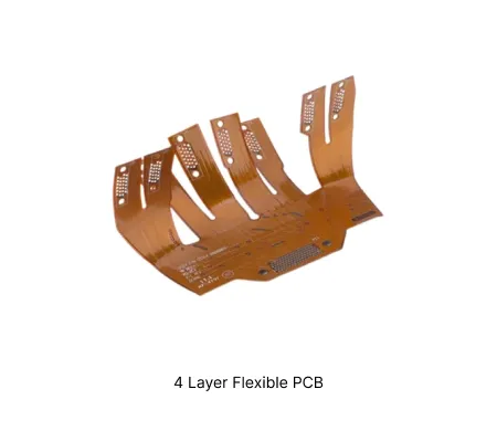
4 Layer Flexible PCB Manufacturing Insights
Discover how AIVON manufactures 4 Layer Flexible PCBs, including multilayer flexible circuit structures, layer alignment control, bending performance, manufacturing challenges, and real production experience from customer orders.
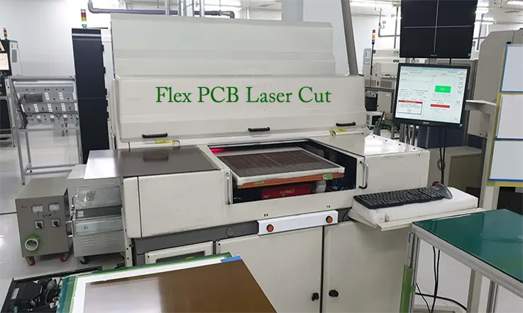
Mastering Flexible PCB Manufacturing: Handling Thin and Bendable Substrates
Learn about flexible PCB manufacturing equipment designed for handling thin, bendable substrates. Gain insights into laser cutting, adhesive bonding, and testing methods to ensure precision and reliability in production.
Real Production Records
| Order ID | PCB Type | Layers | Dimensions | Solder Mask | Surface Finish | Quantity | Action |
|---|---|---|---|---|---|---|---|
| FPC-20260821-065 | Flexible PCB | 4 | 111.25 x 16.75 | Yellow | ENIG (Immersion Gold) | 5 | View detail |
| FPC-20260819-026 | Flexible PCB | 4 | 59.8 x 65.5 | Yellow | ENIG (Immersion Gold) | 25 | View detail |
| FPC-20260810-032 | Flexible PCB | 4 | 357 x 45.8 | Black | ENIG (Immersion Gold) | 1000 | View detail |


