Introduction
Flexible printed circuit boards (PCBs) represent a pivotal advancement in electronic design, enabling compact, lightweight, and adaptable solutions for modern devices. Unlike rigid PCBs, these circuits can bend, fold, and conform to complex shapes, making them essential in industries like aerospace, medical, and consumer electronics. This article explores the core aspects of flexible PCBs, including the materials used, such as polyimide, the detailed fabrication process, sophisticated assembly techniques, and their applications in dynamic bending scenarios. We will also cover flex-rigid PCB design principles and their significance for engineers seeking innovative solutions. Aimed at electrical engineers, this content provides technical insights into optimizing designs with flexible PCB materials while adhering to recognized industry standards for quality and performance.
Benefits of Flexible PCBs: Reducing Costs and Enhancing Reliability
Flexible PCBs are thin, lightweight circuit boards made from pliable materials that allow them to bend and flex without breaking. They serve as a bridge between rigid boards and wiring, offering unique advantages in space-constrained applications. Their importance lies in enabling designs that rigid boards cannot achieve, such as wearable devices, foldable smartphones, and medical implants. By reducing the need for connectors and cables, flexible PCBs lower assembly costs and improve reliability. For engineers, understanding flexible PCB materials and their properties is crucial to meeting design goals. These boards also support dynamic bending, a key feature for applications requiring repeated motion. As technology evolves, their role in compact and efficient designs continues to grow, making them indispensable in modern electronics.
Selecting Flexible PCB Materials for High-Temperature Stability and Dynamic Bending
Flexible PCB materials form the foundation of their unique properties. For a deeper understanding of the materials used for making flexible PCBs, including their specific properties and applications, refer to our dedicated guide. The most common substrate is polyimide, known for its excellent thermal stability, chemical resistance, and flexibility. Polyimide flexible PCBs can withstand high temperatures, often up to 260 degrees Celsius during soldering processes, as per industry guidelines. This makes them suitable for harsh environments like automotive and aerospace systems. Other materials, such as polyester, are used for less demanding applications due to their lower cost but reduced thermal tolerance.
Conductive layers typically consist of copper, either rolled annealed or electrodeposited, to ensure flexibility without cracking. Adhesives or adhesive-less constructions bond these layers, with the latter preferred for thinner, more flexible designs. Coverlays, often made of polyimide with adhesive, protect the circuitry while maintaining pliability. For engineers, selecting the right combination of materials is critical to balance flexibility, durability, and cost.
Industry standards, such as IPC-6013D, provide guidelines for material selection and performance criteria for flexible printed boards. These standards ensure that materials meet the necessary mechanical and electrical properties for reliable operation. Understanding material behavior under stress, especially in dynamic bending flexible PCBs, helps engineers predict long-term performance and avoid failures in critical applications.
The Flexible PCB Fabrication Process: Step-by-Step Manufacturing Stages
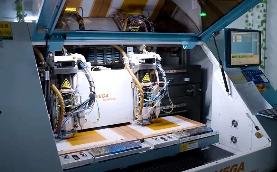
The flexible PCB fabrication process differs significantly from that of rigid boards due to the unique materials and design requirements. It begins with the preparation of the base material, typically a polyimide film, which is cleaned and treated to ensure proper adhesion of conductive layers. This intricate process relies on specialized flexible PCB manufacturing equipment designed for handling thin and bendable substrates with precision. A thin copper foil is then laminated onto the substrate, often using heat and pressure, to form the conductive pathways.
Etching follows, where unwanted copper is removed to create the desired circuit pattern. This step requires precision to avoid damaging the thin, flexible substrate. A coverlay or protective layer is applied to insulate and shield the traces from environmental factors. For multilayer flexible PCBs, additional layers are aligned and bonded, ensuring accurate registration to maintain signal integrity.
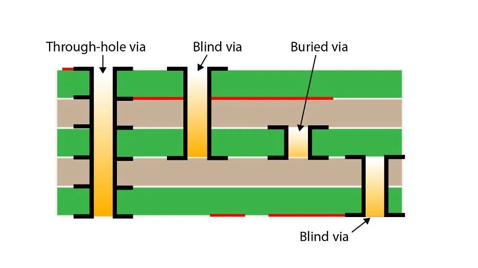
Drilling and plating are performed for vias, if needed, though flexible PCBs often minimize through-holes to preserve flexibility. Final steps include cutting the board to shape and testing for electrical performance. Standards like IPC-A-600K guide the acceptability of printed boards, ensuring quality at each stage of the flexible PCB fabrication process. Engineers must account for material shrinkage and stress during fabrication to prevent defects.
Testing for dynamic bending flexible PCBs involves repeated flex cycles to simulate real-world use. This ensures the board can endure mechanical stress without trace cracking or delamination. Adhering to fabrication guidelines is vital for achieving consistent results, especially in high-reliability applications.
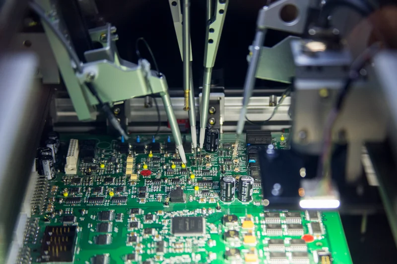
Specialized Flexible PCB Assembly Techniques: SMT, Soldering, and Handling
After fabrication, the Flexible PCB Assembly Techniques present their own set of considerations. Unlike rigid PCBs, the pliable nature of flexible circuits requires specialized handling and processes to prevent damage. Components are typically mounted using surface-mount technology (SMT), but due to the substrate's heat sensitivity, reflow profiles must be carefully controlled, often utilizing lower peak temperatures or selective soldering. Adhesives and underfills play a crucial role in enhancing the mechanical integrity of components on flexible substrates, especially in dynamic bending applications. For a comprehensive guide on various flexible PCB assembly techniques, including best practices and common challenges, explore our detailed article. The final assembly must undergo rigorous testing to ensure both electrical functionality and mechanical durability, particularly when considering the board's intended flex cycles and environmental exposure.
Flexible PCB Design: Layout Principles and IPC-2223D Guidelines
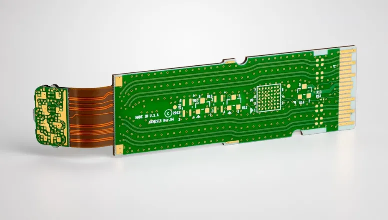
Flexible PCB design combines the benefits of both flexible and rigid circuits into a single board, offering structural stability and adaptability. These designs typically feature rigid sections for mounting components and flexible sections for bending or connecting different parts of a device. This hybrid approach is ideal for compact systems where space and weight are critical constraints.
Key considerations in flexible PCB design include defining the bend radius, which determines how tightly the flexible portion can fold without damaging traces. Industry standards, such as IPC-2223D, provide detailed guidelines on bend radius calculations and stress management. Engineers must also ensure proper layer stackup, balancing the number of flexible and rigid layers to meet electrical and mechanical needs.
Trace routing in flexible areas requires careful planning to avoid stress concentration points. Widening traces or using teardrop shapes at vias can enhance durability. Stiffeners may be added to support component mounting in flexible zones. Material selection is equally important, as polyimide flexible PCB substrates must align with the rigid materials to prevent delamination during thermal cycles.
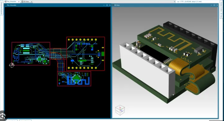
Signal integrity must be maintained across transitions between rigid and flexible regions. High-speed designs may require controlled impedance, necessitating precise material and thickness choices. By following established design rules, engineers can create reliable flex-rigid PCBs for complex applications.
Ensuring Reliability in Dynamic Bending Flex PCBs: Stress Management and Durability
Dynamic bending flexible PCBs are designed for applications where repeated flexing occurs, such as in foldable devices or robotic systems. Unlike static flex designs, which bend once during installation, dynamic bending requires materials and layouts that withstand thousands of cycles without failure. Polyimide flexible PCBs are often the material of choice due to their resilience under mechanical stress.
Key factors in designing for dynamic bending include minimizing the bend radius while ensuring trace integrity. Copper traces should be oriented perpendicular to the bend axis to reduce stress. Adding strain relief features, such as curved traces or mesh patterns, can further enhance durability. Standards like IPC-6013D outline testing methods for flex endurance, providing benchmarks for performance.
Engineers must also consider environmental factors, such as temperature and humidity, which can affect material properties during bending. Thermal expansion mismatches between layers can lead to cracking, so selecting compatible materials is essential. Thorough testing under simulated conditions ensures that dynamic bending flexible PCBs meet the demands of their intended use.
Flexible PCB Applications: From Consumer Electronics to Wearable Health Tech
Flexible PCBs find applications across a wide range of industries due to their adaptability and compact form. In consumer electronics, they enable slim designs in smartphones, tablets, and wearable devices. Medical equipment, such as hearing aids and implantable devices, relies on flexible PCBs for their small size and biocompatibility. Aerospace systems use them for weight reduction and reliability in harsh conditions.
Automotive electronics benefit from flexible PCB designs in control modules and sensors, where space constraints and vibration resistance are critical. Industrial automation employs flexible PCBs in robotic arms and moving parts, leveraging their dynamic bending capabilities. Each flexible PCB application demands specific material and design choices to meet performance requirements.
Beyond these broad categories, specific niche applications are increasingly leveraging the unique benefits of flexible PCBs.
Flexible PCBs for Smart Eyewear
The burgeoning field of smart wearables, particularly eyewear, heavily relies on flexible PCB technology. Flexible PCBs for Smart Eyewear are critical for integrating sophisticated electronics into unobtrusive, comfortable frames, enabling features like augmented reality displays, biometric sensors, and communication modules without adding bulk. Their ability to conform to complex, non-planar surfaces is indispensable here. To delve deeper into the design, materials, and assembly challenges specific to flexible PCBs for smart eyewear, explore our dedicated article.
Flexible PCB Design for Wearable Health Tech
Similarly, in the rapidly expanding healthcare sector, the Flexible PCB Design for Wearable Health Tech is revolutionizing patient monitoring and diagnostics. From continuous glucose monitors to advanced vital sign trackers and smart patches, flexible PCBs enable direct skin contact, lightweight profiles, and the necessary resilience for daily wear. Their biocompatibility and ability to integrate multiple sensor types within a single flexible substrate are key differentiators. Engineers developing solutions in this space require specialized knowledge, as detailed in our advanced guide on flexible PCB design for wearable health tech, covering everything from material selection to advanced integration strategies.
By tailoring flexible PCB materials and fabrication techniques, engineers can address the unique challenges of each sector. Standards like ISO 9001:2015 ensure consistent quality in production, supporting the reliability needed for critical applications. Understanding the end-use environment is key to selecting the right flexible PCB configuration.
Conclusion
Flexible PCBs offer unparalleled advantages in modern electronic design, from their adaptable materials like polyimide to their complex fabrication processes and sophisticated assembly techniques. They enable innovative solutions through flex-rigid PCB design and dynamic bending capabilities, meeting the needs of diverse industries, including cutting-edge applications in smart eyewear and wearable health tech. Engineers can optimize performance by selecting appropriate flexible PCB materials and adhering to industry standards during design and manufacturing. As technology advances, the role of flexible PCBs will only expand, driving efficiency and creativity in electrical engineering. This exploration of their materials, fabrication, assembly, and applications provides a foundation for tackling the challenges of next-generation designs.
FAQs
Q1: What are the key flexible PCB materials used in high-temperature applications?
A1: Polyimide is the primary material for high-temperature environments in flexible PCBs. It offers thermal stability and can endure soldering temperatures without degrading. Often used in aerospace and automotive sectors, polyimide flexible PCBs provide reliable performance under stress. Engineers select it for its balance of flexibility and durability, ensuring long-term operation in demanding conditions.
Q2: How does the flexible PCB fabrication process differ from rigid PCB manufacturing?
A2: The flexible PCB fabrication process focuses on pliable substrates like polyimide, requiring specialized lamination and etching techniques. Unlike rigid boards, it minimizes through-holes to maintain flexibility. Coverlays replace solder masks for protection, and precise alignment is critical for multilayer designs. Standards like IPC-A-600K guide quality control to ensure defect-free production.
Q3: What factors should engineers consider in flex-rigid PCB design?
A3: In flex-rigid PCB design, engineers must define bend radius, ensure layer compatibility, and maintain signal integrity. Trace routing in flexible areas needs stress relief features to prevent cracking. Standards like IPC-2223D offer guidelines for stackup and bending limits. Material selection and thermal expansion matching are also crucial for reliability.
Q4: How do dynamic bending flexible PCBs perform in wearable technology?
A4: Dynamic bending flexible PCBs are ideal for wearables due to their ability to withstand repeated flexing. They use durable materials like polyimide to handle motion without trace failure. Designs incorporate strain relief to enhance longevity. Testing per IPC-6013D ensures they meet endurance requirements for continuous use in fitness trackers and smartwatches.
Q5: What are the primary considerations for flexible PCB assembly?
A5: Flexible PCB assembly requires careful attention to component placement, thermal management during soldering, and stress relief for traces and components. Due to the substrate's flexibility and often thinner nature, specialized low-temperature solders or precise reflow profiles are used. Adhesives and underfills are crucial for mechanical stability. Thorough testing, including for dynamic flexing, ensures the assembled board meets performance and reliability standards.
References
IPC-6013D — Qualification and Performance Specification for Flexible and Rigid-Flex Printed Boards. IPC, 2017.
IPC-A-600K — Acceptability of Printed Boards. IPC, 2020.
IPC-2223D — Sectional Design Standard for Flexible/Rigid-Flex Printed Boards. IPC, 2016.
ISO 9001:2015 — Quality Management Systems. ISO, 2015.