Ultra-thin 2-layer flexible PCBs (FPCs) at 0.2 mm thickness demand precise CAM engineering review due to their unique material behavior and processing limitations. This real production case involves a 288 × 95 mm 2-layer FPC using 1oz copper and OSP surface finish, where multiple conflicts arose between customer design data and standard flexible circuit manufacturing capabilities. Issues centered on panelization tabs, asymmetric coverlay application, solder mask opening compensation, and process edge stiffening.
As a senior CAM engineer, I have reviewed hundreds of FPC orders and consistently see how flexible material properties amplify small design decisions into major manufacturability risks. Our team raised several EQs to prevent common FPC failures such as tearing during handling, registration misalignment, and poor solderability. This article details the actual engineering questions, the reasoning behind them, potential risks if ignored, and how we resolved them.
Order Overview
The order specified a 2-layer flexible PCB ( #FPC-20260410-059 ) with 0.2 mm finished thickness, 1oz copper on both layers, and pressed copper material. Board size was 288 × 95 mm, panelized by the customer as 5×1 with V-cut separation. Surface finish was OSP, with white coverlay on top and black legend. Minimum hole size was 0.3 mm. The design required full flying probe testing and laser forming. Quantity was 25 pcs (5 sets). Delivery target was 9 days.
This ultra-thin construction combined with asymmetric coverlay and customer panelization created several process challenges typical for flexible circuits, particularly in handling, registration, and coverlay application.
Main Engineering Questions Found During CAM Review
Panelization and Connection Tabs for Flexible Board Processing
We noticed the customer panelization required special handling for flexible material. Our engineer suggested adding multiple 1.0 mm connection tabs along the outline to maintain panel integrity during processing. This is standard practice for FPC panelization to prevent individual boards from separating prematurely during laser cutting and handling.
Figure 1: adding multiple 1.0 mm connection tabs along the outline
If ignored, loose boards in the panel could shift during coverlay lamination or laser forming, causing registration errors or even tearing of the thin polyimide substrate. We have seen such cases result in significant scrap and production delays. The customer confirmed acceptance of our proposed flexible connection method.
Asymmetric Coverlay Configuration (Top White, Bottom Open)
The design called for white coverlay on the top layer while leaving the bottom layer fully open without solder mask. After reviewing the stackup, we confirmed this asymmetric structure was feasible but required careful lamination process adjustments. Our CAM team identified potential risks in bow and twist due to unbalanced material stress on such a thin 0.2 mm board.
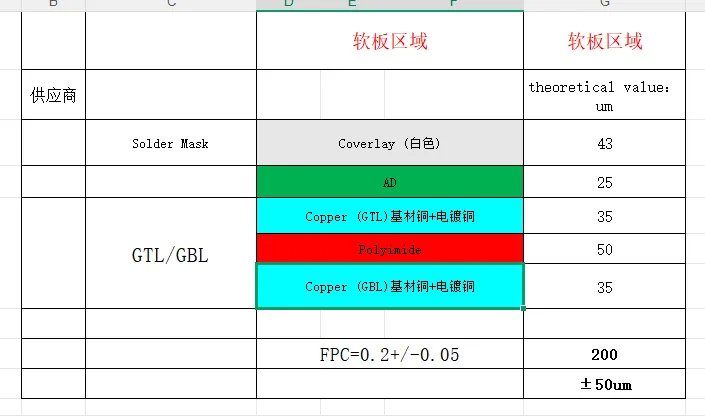
Figure 2: white coverlay on the top layer while leaving the bottom layer fully open without solder mask
If not validated, unbalanced coverlay could lead to excessive board warpage, making assembly difficult and potentially causing open circuits or component misalignment after reflow. We proposed the adjusted stackup and received customer confirmation to proceed.
Solder Mask Opening Size Optimization
The original coverlay openings were significantly larger than the stencil pads. We recommended adjusting the openings to match stencil size with only 0.05 mm single-side compensation. This change ensures better solder paste registration and prevents solder bridging on fine-pitch features.
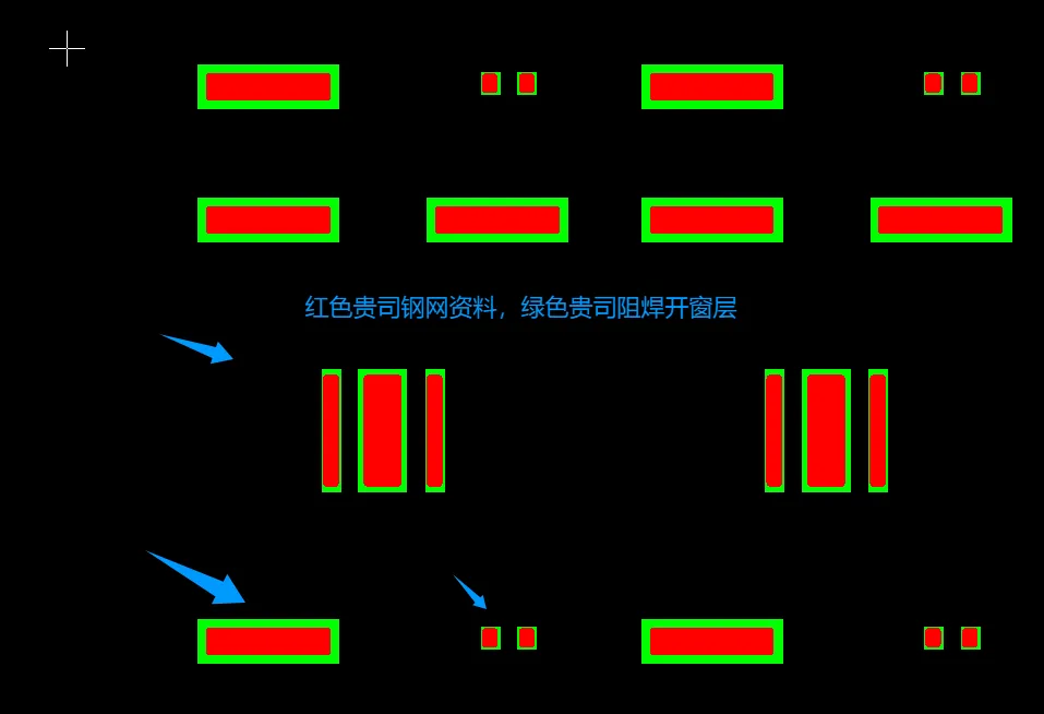
Figure 3: original coverlay openings were significantly larger than the stencil pads
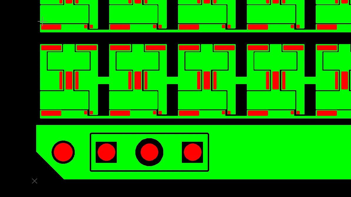
Figure 4: solder mask opening size optimization
Without this adjustment, oversized openings could cause poor solderability, excessive solder paste volume, or bridging, leading to assembly defects and rework. In thin FPCs, such issues are harder to correct and often result in higher yield loss. Our team updated the production files after customer approval.
Process Edge Stiffening and Date Code Marking
We suggested adding copper pour on both sides of the process edges to act as stiffeners for better panel handling. Additionally, the customer requested a date code (year-week only) on the process edge. These were minor but important for production traceability and process stability.
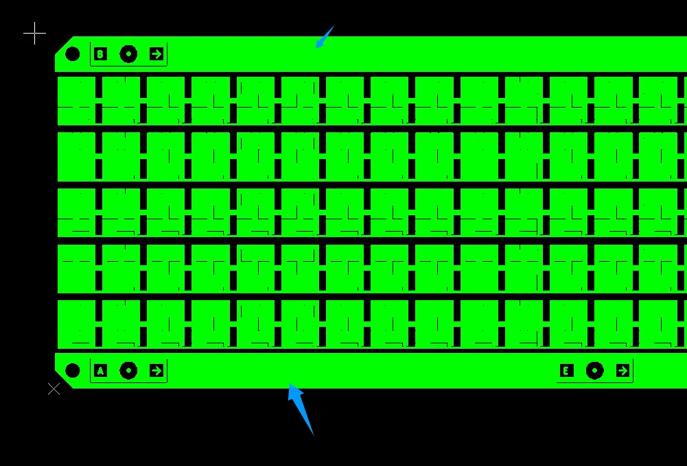
Figure 5: adding copper pour on both sides of the process edges
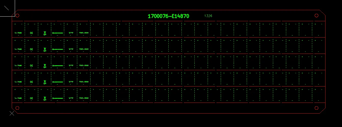
Figure 6: a date code (year-week only) on the process edge
Manufacturing Risks and DFM Insights
Flexible PCBs are particularly sensitive to unbalanced constructions. Designers frequently specify asymmetric coverlay without considering the resulting bow and twist on thin substrates. Oversized coverlay openings relative to stencil pads are another common oversight that directly impacts SMT yield.
Panelization for FPCs requires specific connection tab strategies that differ from rigid boards. If EQs are ignored, risks include material tearing during laser forming, warpage leading to assembly failure, poor solder joint reliability, and increased scrap rates. Early clarification prevents costly multiple revision cycles and production delays.
How the Engineering Team Resolved the Issues
We prepared a comprehensive EQ package with annotated images showing proposed connection tabs, coverlay adjustments, and edge copper. After customer confirmation on all points, our team updated the production files, optimized the laser cutting program, and verified the asymmetric stackup for lamination stability. These steps ensured the thin FPC panel could be processed reliably.
Final Manufacturing Outcome
All engineering questions were clarified and confirmed by the customer. Manufacturing parameters were adjusted accordingly, and the order was released for production with optimized files for flexible circuit processing.
Key Takeaways for PCB Designers
- Clearly define coverlay requirements for each layer in FPC designs, especially when asymmetric, and consult the manufacturer on potential warpage risks for ultra-thin boards.
- Match coverlay openings closely to stencil pad sizes with minimal compensation to ensure good SMT performance.
- Specify panelization details including connection tab requirements for flexible boards to avoid handling issues.
- Include process edge stiffening (copper pour) where panel stability is needed during manufacturing.
- Provide clear instructions for date codes or markings, including exact content and location.
- Submit complete fabrication notes distinguishing design intent from manufacturing allowances for FPCs.
- Request DFM review early for thin flexible designs to minimize EQs and lead time.
FAQ
Q1: Why is asymmetric coverlay challenging on 0.2 mm FPCs?
A1: Unbalanced material layers can cause significant bow and twist due to different thermal expansion and shrinkage rates during lamination and cooling, affecting assembly and reliability.
Q2: What are the risks of oversized coverlay openings?
A2: Excessive opening sizes lead to too much solder paste, bridging, or poor joint formation during SMT, increasing assembly defects and reducing yield.
Q3: Why do FPCs need special connection tabs in panelization?
A3: Thin flexible material can shift or tear easily without proper tabs to hold boards securely during processing and laser forming.
Q4: Should designers add copper on process edges for FPCs?
A4: Yes, in many cases it acts as a stiffener, improving panel stability and registration during manufacturing steps.
Q5: How important is matching coverlay to stencil openings?
A5: Critical for reliable solder paste deposition and to avoid defects. Manufacturers often recommend minimal compensation based on actual process capabilities.