In this real-world engineering case from our CAM department, we reviewed a standard 4-layer FR-4 board (#FR4-20260505-078) destined for 200 pieces production. What started as a routine 1.6mm TG150 OSP board quickly revealed several manufacturability gaps between the customer's design intent and our production capabilities. Our team raised multiple EQs to prevent potential defects before releasing the job to the shop floor.
Introduction
4-layer PCBs remain among the most common yet deceptively challenging orders we process. With moderate complexity, designers often assume standard DFM rules will apply without issue. However, mixed via treatments, conflicting mechanical layers, and tight edge clearances frequently surface during CAM review. In this case, the combination of V-CUT combined with routing panelization (1x2), 0.3mm minimum holes, and inconsistent Gerber data triggered several clarification requests.
Our CAM engineers perform detailed file analysis to bridge the gap between design software output and actual fabrication constraints. Ignoring these details can lead to exposed copper, plating defects, or assembly failures. This case study walks through the key issues we identified, the risks involved, and how we resolved them to ensure a smooth production run.
Order Overview
This was a 4-layer board using FR-4 material (equivalent to KB-6165F) with TG150 rating and 1.6mm finished thickness. Copper weight was 1oz on both inner and outer layers. Surface finish specified OSP, with green solder mask on both sides and no silkscreen. Minimum hole size was 0.3mm, and the board measured 119mm x 210mm. Panelization used a 1x2 array with V-CUT combined with routing for depanelization. The order called for 200 pieces (100 sets), 100% flying probe testing, and a tight 2-day delivery.
Stackup followed a standard symmetrical configuration with no special impedance requirements noted. While the parameters looked straightforward on paper, the provided Gerber and mechanical data contained several inconsistencies that required customer confirmation before proceeding with tooling and production.
Main Engineering Questions Found During CAM Review
1. Inconsistent Via Tenting (Open Window vs. Cover Oil)
Our engineer noticed that in the Gerber files, some vias had solder mask openings while others were designed to be tented. However, the system order parameters clearly specified via cover oil (tented vias). We raised this EQ to confirm the intended manufacturing approach for via treatment.
Figure 1: Some vias had solder mask openings while others were designed to be tented.
We noticed this discrepancy during the solder mask layer comparison. Mixed via treatment can create serious issues in high-volume runs. If left unresolved and we followed the Gerber exactly, some vias would remain exposed while others were covered, leading to inconsistent soldering behavior during assembly. In the worst case, exposed vias near high-density areas could cause solder bridging or flux residue problems, resulting in assembly yield loss or field reliability issues.
According to typical IPC-A-600 acceptability criteria, uniform via treatment is preferred for reliable performance. Our team recommended following the system order for full tenting to maintain process consistency with the OSP finish. The customer confirmed the tenting requirement, allowing us to adjust the solder mask data accordingly.
2. Routing Layer Conflict (GM2 vs GM3) and Drill Size Mismatches
Multiple EQs focused on mechanical/routing layers. The customer provided conflicting GM2 and GM3 data for slot and outline routing. Our standard practice is to clarify which layer should take precedence and ignore the secondary one.
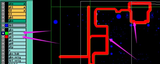
Figure 2: Routing slot layer in accordance with GM3 data
We also pointed out areas where drill layer sizes did not match the mechanical data.
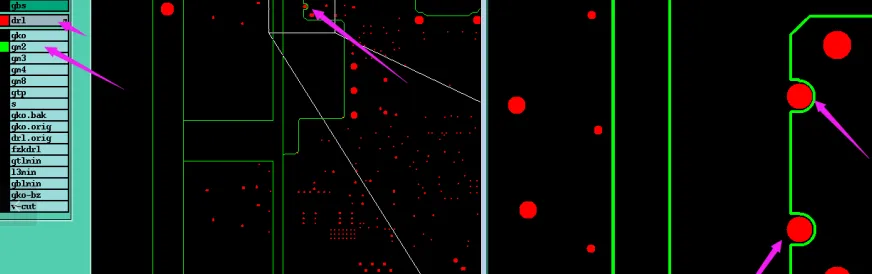
Figure 3: Drill layer sizes do not match the GM2 layer's.
After reviewing the stackup and mechanical files, we found that following the wrong layer could result in incorrect slot dimensions or misplaced routing paths. If ignored, this would lead to dimensional inaccuracies during depanelization, potentially causing board edge damage or fit issues in the final assembly. Our CAM engineer confirmed that standardizing on the primary routing layer resolved the conflict and aligned with the V-CUT + routing panelization specified (1x2 array).
We also addressed PDF annotations that contradicted the primary fabrication data. These were ignored in favor of the system order parameters, as is our protocol for maintaining production integrity.
3. Critical Edge Clearance Issue Near V-CUT
One of the most manufacturability-critical findings was pads located too close to the board edge in the V-CUT area. We raised an EQ asking for confirmation on how to handle the potential copper exposure during scoring.
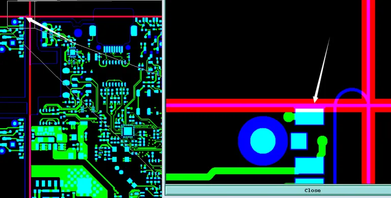
Figure 4: Pads are located too close to the board edge in the V-CUT area.
Our engineer suggested adjusting the copper clearance because we noticed the V-CUT area was too close to exposed copper features. In V-CUT processing, the scoring blade removes material along the panel lines. When copper pads or traces sit too close, the result is exposed copper on the finished board edge after depanelization.
If this had been ignored and production continued without clarification, exposed copper could appear after depanelization, potentially causing edge shorting during assembly or long-term corrosion risks, especially with OSP finish which offers limited edge protection. Based on IPC-2221 spacing guidance for mechanical operations, we recommended either moving the features inward or adding protective measures where possible. The customer accepted our proposed adjustment to prevent these defects.
4. Solder Mask Openings Exposing Traces and Stamp Hole Spacing
Additional issues included solder mask openings that exposed traces in certain areas and overly tight stamp (mouse bite) hole spacing that prevented proper linking.
For the mask openings, we confirmed acceptance of the file design after review.
Figure 5: Solder mask openings that exposed traces in certain areas
For the stamp holes, we adjusted by removing one perforation to ensure clean depanelization without risking board cracking or incomplete separation.
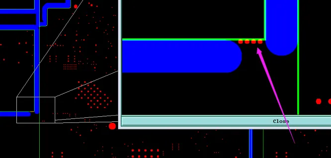
Figure 6: Overly tight stamp (mouse bite) hole spacing

Figure 7: Suggested removing one perforation
5. Large Hole Type Clarification
For a prominent central hole, we sought confirmation on whether it should be treated as a plated through-hole or component hole, noting the asymmetric solder mask treatment (open on top, covered on bottom).
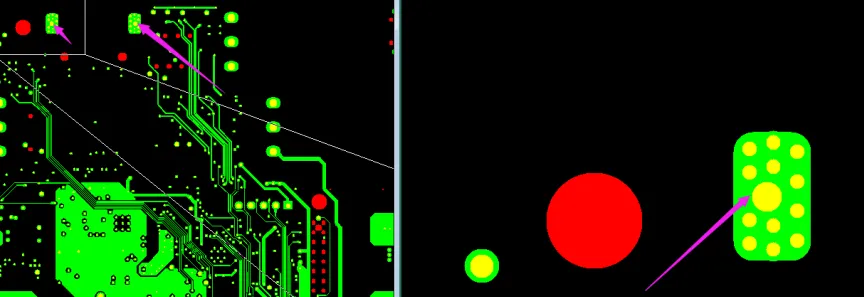
Figure 8: Central hole on the pad
Suggested EQ Categories
File & Manufacturing Data Issues
- Conflicting Gerber vs. system order parameters for via tenting
- PDF annotation conflicts with primary data
Panelization & Process Optimization
- V-CUT edge clearance and copper exposure risk
- Stamp hole spacing and linking problems
- Routing layer standardization
Hole & Tolerance Issues
- Drill vs. mechanical layer size mismatches
- Large hole classification (via vs. component)
Manufacturing Risks and DFM Insights
This case highlights common pitfalls in 4-layer designs: designers often overlook how panelization methods interact with copper features. V-CUT is efficient for rectangular boards but unforgiving of edge proximity. Ignoring the clearance would likely cause cosmetic defects at minimum and functional shorts at worst.
Via tenting inconsistencies can lead to variable solder volume, increasing the chance of tombstoning or insufficient barrel fill during reflow. Conflicting mechanical layers risk wrong outline dimensions, leading to scrap boards when panels are routed or scored incorrectly.
From a CAM perspective, these issues demonstrate why pre-production EQs exist — not to delay projects, but to protect yield. In this order, proactive clarification prevented potential delamination risks near slots, copper peeling at edges, and open circuits from poor via plating consistency.
How the Engineering Team Resolved the Issues
Our engineering team suggested standardizing on the primary mechanical layer for all routing operations after careful layer comparison. For the edge clearance, we proposed minor copper pullback in the affected areas to maintain V-CUT integrity without major redesign. Via tenting was uniformly applied per the order parameters.
We also optimized stamp hole placement to ensure reliable panel separation. All changes were documented and shared with the customer for approval before updating the production files. This workflow minimized risk while respecting the original design intent as closely as possible.
Final Manufacturing Outcome
After receiving customer confirmations on all EQ points, the CAM files were finalized. Adjustments were implemented for consistent via tenting, routing layers, and edge clearances. The job was approved for production with the optimized panelization and testing parameters. The board successfully moved into fabrication without further issues.
Key Takeaways for PCB Designers
- Ensure via tenting intent is clearly documented in both Gerber files and fabrication notes — inconsistencies trigger mandatory EQs.
- Provide a single authoritative mechanical layer for routing and slots; avoid overlapping layers with conflicting data.
- Maintain adequate copper-to-V-CUT clearance (typically greater than 0.5mm depending on process) to prevent edge exposure.
- Verify stamp hole spacing allows proper webbing for clean depanelization.
- Cross-check drill sizes against mechanical layers before release.
- Clearly specify asymmetric mask requirements for non-standard holes.
- Use consistent layer naming and avoid relying solely on PDF callouts for critical dimensions.
- Consider panelization method early in the design phase, especially when mixing V-CUT and routing.
FAQ
Q1: Why do PCB factories require confirmation on via tenting when files show mixed openings?
A1: Mixed tenting creates process variability in solder mask application and can lead to inconsistent assembly behavior. Factories standardize based on order parameters to ensure reliability and avoid defects like solder wicking into vias.
Q2: What happens if V-CUT clearance is insufficient?
A2: Exposed copper appears on board edges after scoring, risking shorts, corrosion (especially with OSP), and assembly handling problems. This often leads to cosmetic rejection or functional failures.
Q3: Why prioritize one mechanical layer over another?
A3: Conflicting layers can cause the wrong routing path or slot size to be used, resulting in dimensional errors and scrapped panels. Standardizing prevents manufacturing ambiguity.
Q4: How does stamp hole spacing affect depanelization?
A4: Insufficient spacing prevents proper perforation linking, making boards hard to separate cleanly and risking cracks or rough edges. Adjustment ensures reliable mouse-bite performance.
Q5: Should designers always follow factory recommendations on edge features?
A5: Yes, when V-CUT or routing is involved. Factories have process-specific tolerances based on equipment and material behavior that generic design rules may not fully capture.
Q6: What is the benefit of early EQ communication in PCB orders?
A6: It prevents production delays, reduces scrap risk, and avoids costly re-runs. Clarifications allow DFM optimizations that improve overall yield and delivery performance.