Thin 4-layer PCBs with 0.8 mm finished thickness present significant manufacturing challenges, especially when countersink holes are involved. This real engineering case examines a compact 4-layer FR4 board (65.02 × 287.27 mm) where multiple data inconsistencies and critical DFM issues surfaced during CAM review. The primary concerns revolved around countersink specifications, hole file offsets, layer polarity, and edge proximity risks.
As a senior CAM engineer with over 15 years of experience, I have seen how insufficient documentation for mechanical features like countersinks can quickly escalate into production failures on thin multilayer boards. Our team raised several EQs to clarify ambiguities and prevent irreversible defects. This article details the actual issues discovered, the manufacturing reasoning behind our questions, potential consequences if ignored, and the resolution process.
Order Overview
This was a 4-layer FR4 PCB ( #FR4-20260420-121 ) using TG130 material, 0.8 mm total thickness, and 1oz copper on inner and outer layers. The board dimensions were 65.02 × 287.27 mm with 4 mm process edges on top and bottom. Surface finish was HASL, with cold white solder mask on both sides and yellow legend. Minimum hole size was 0.3 mm, requiring 100% flying probe testing. The order quantity was 5 pcs (5 sets), with routing separation and customer-provided panelization data. Delivery was urgent at 3 days.
The combination of thin overall thickness, multilayer construction, and unspecified countersink requirements created a tight process window that demanded thorough CAM validation before releasing to production.
Main Engineering Questions Found During CAM Review
Countersink Hole Specifications and Depth Conflict on 0.8 mm Board
The customer order indicated countersink holes, but no specific positions, diameters, or depths were provided in the fabrication notes or drawings. After calculation based on standard practices, our engineer determined that achieving the typical countersink depth of 0.85 mm ± 0.2 mm on a 0.8 mm thick board would risk penetrating too deeply.
Figure 1: customer order indicated countersink holes
Figure 2: no specific positions, diameters, or depths were provided in the fabrication notes or drawings
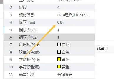
Figure 3: 0.8 mm thick board
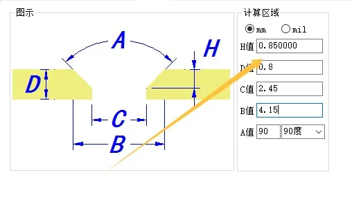
Figure 4: typical countersink depth of 0.85 mm ± 0.2 mm on a 0.8 mm thick board
We noticed this discrepancy immediately during stackup review. If ignored, the countersinking process could cause hole breakout on the back side, damage to L1 and L2 copper layers, or complete board thinning leading to structural weakness. In the worst case, this results in scrap boards, poor component seating, or mechanical failure during assembly. According to IPC-6012 guidelines for mechanical features, such depth conflicts on thin boards frequently lead to unreliable plating and reduced reliability. We requested exact parameters and proposed safer alternatives.
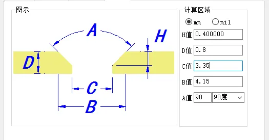
Figure 5: enlarge the small hole to 3.35 mm for manufacturing
Countersink Hole Proximity to Board Edge
Several countersink holes were positioned very close to the board edge. Our CAM team identified that routing the outline could cause breakout or chipping at the hole edges due to limited material support on this thin panel.
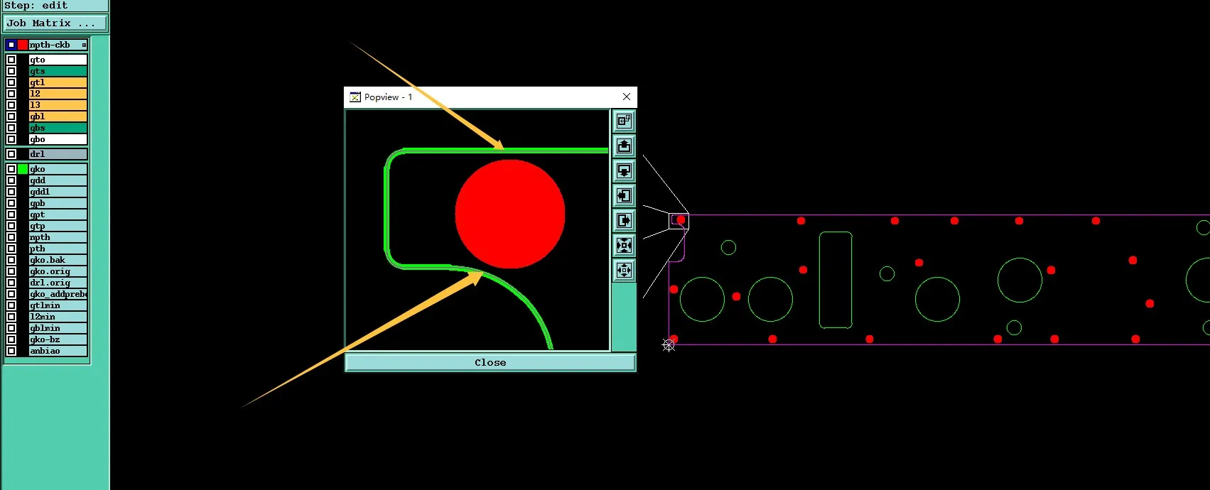
Figure 6: several countersink holes were positioned very close to the board edge
Proceeding without adjustment risked irregular hole edges, exposed copper, or weakened board integrity after depanelization. We have observed similar configurations result in cosmetic defects failing IPC-A-600 acceptance and functional issues during connector or screw installation. Our engineer suggested confirming positions and potentially increasing clearance to maintain manufacturability.
Hole File Offset and Drawing Size Mismatch
We detected offsets between the provided hole file and actual drill symbols. Additionally, the hole drawing did not match the production data dimensions. These mismatches required immediate clarification to avoid misdrilling across layers.
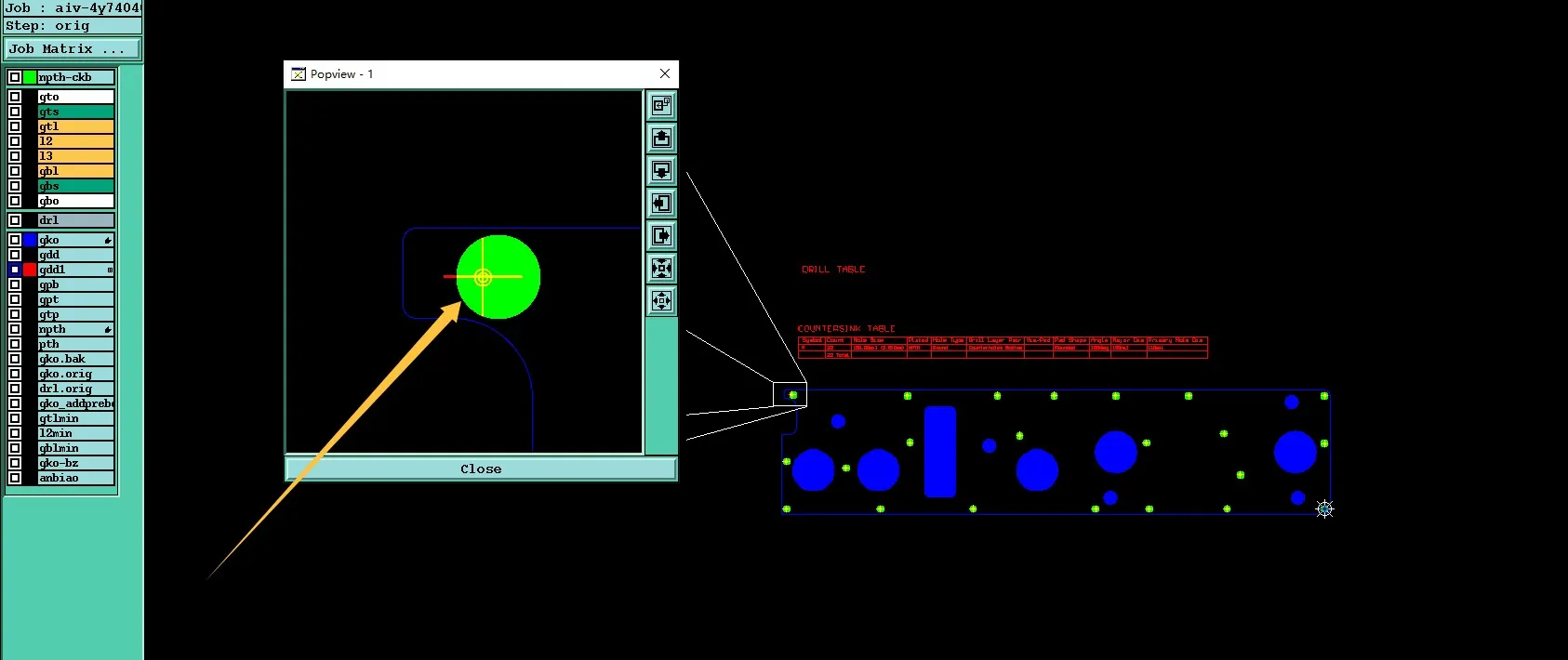
Figure 7: offsets between the provided hole file and actual drill symbols
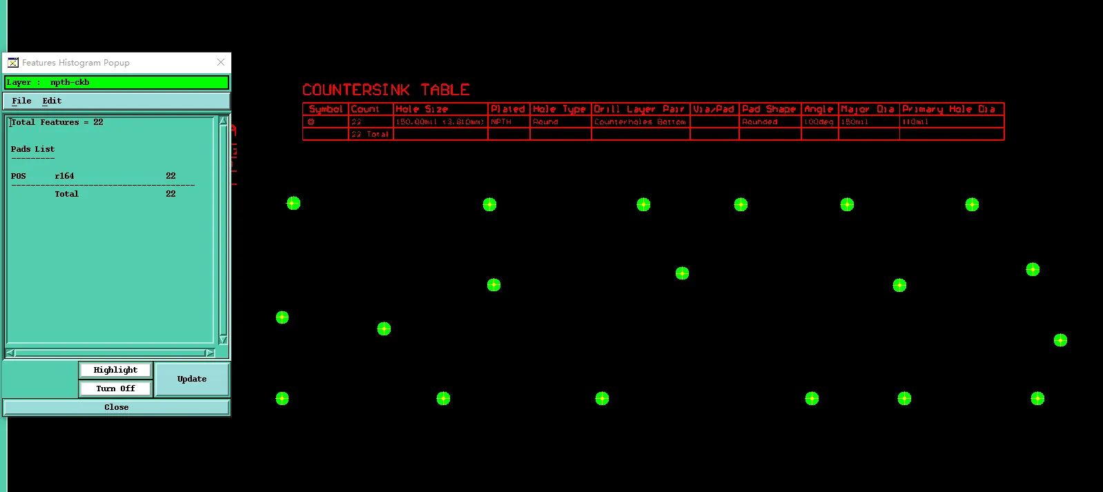
Figure 8: hole drawing did not match the production data dimensions
If unaddressed, this could lead to misaligned holes, open circuits, or short circuits between layers. On a 4-layer board, such registration errors often cause significant yield loss and require costly rework.
Layer Polarity and Legend Marking Confirmation
L3 and L4 layers showed positive text orientation that needed verification. We also questioned a potential special marking after "SN" on the bottom legend layer. These were confirmed as minor but essential for correct fabrication output.
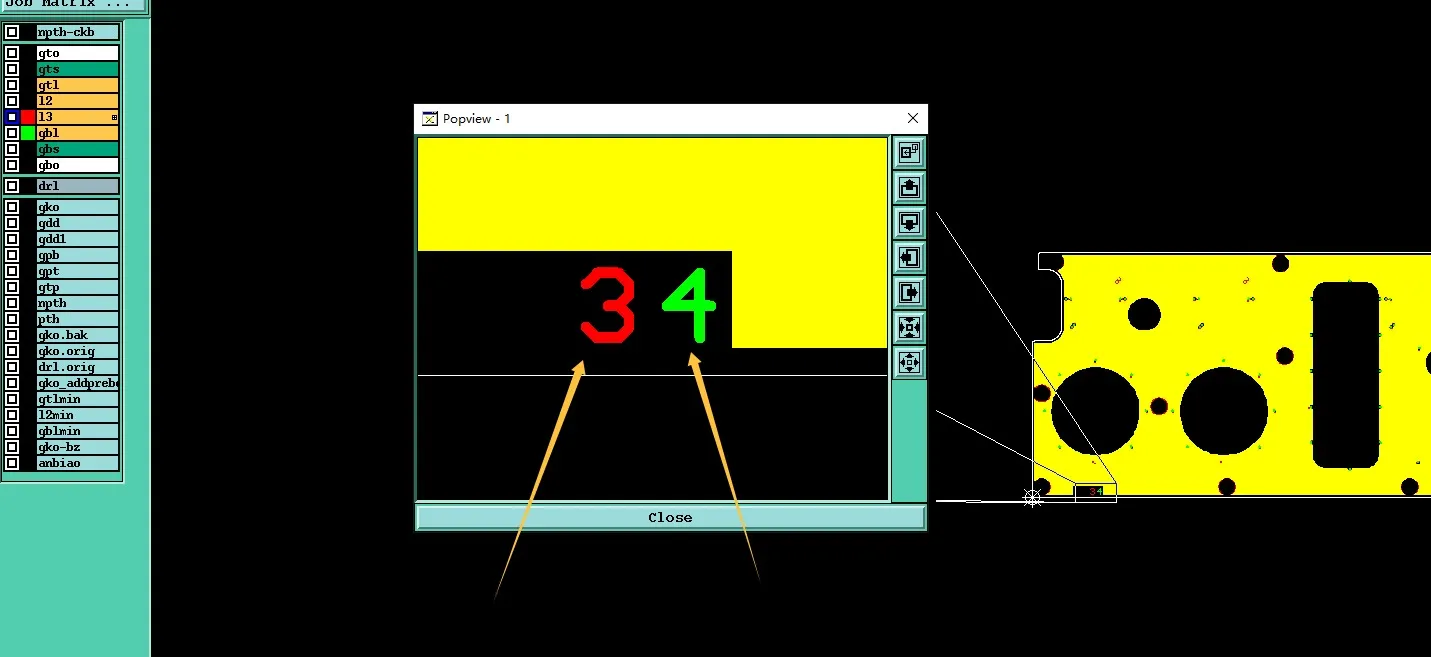
Figure 9: L3 and L4 layers showed positive text orientation
Manufacturing Risks and DFM Insights
Thin multilayer boards (under 1.0 mm) have limited tolerance for mechanical operations like countersinking. A common customer mistake is specifying countersinks without detailed drawings or depth parameters, assuming the factory can infer intent. On 0.8 mm boards, the remaining material after countersinking becomes critically thin, amplifying risks of copper damage and breakout.
Hole file inconsistencies and poor edge clearances further compound issues during routing. Ignoring these EQs typically leads to high scrap rates, production delays, increased costs from re-paneling, and potential field failures due to compromised mechanical strength. This case illustrates why CAM review is non-negotiable for thin, high-layer-count designs with special mechanical features.
How the Engineering Team Resolved the Issues
We compiled detailed EQs with annotated screenshots highlighting offsets, depth calculations, and edge risks. After customer clarification on countersink parameters and confirmation of layer polarity, our team adjusted the drill programs, optimized routing paths to increase edge clearance where possible, and verified all files for consistency. Production numbering was added as requested.
These DFM optimizations reduced mechanical stress during routing and ensured the countersink depths stayed within safe limits for the 0.8 mm thickness.
Final Manufacturing Outcome
All engineering questions received customer confirmation. Manufacturing files were updated with corrected parameters, and the order was approved for production after final CAM validation.
Key Takeaways for PCB Designers
- Always provide detailed drawings and specifications for countersink holes, including exact locations, diameters, depths, and tolerances.
- Avoid placing mechanical features like countersinks too close to board edges on thin PCBs to prevent breakout during routing.
- Ensure drill files, drawings, and Gerber layers are fully consistent before submission to eliminate offsets and mismatches.
- Clearly specify layer polarity (positive/negative) for all layers, especially inner layers.
- Include complete fabrication notes covering all special mechanical requirements when ordering thin multilayer boards.
- Request early DFM review for designs with countersinks or other depth-critical features on boards under 1.0 mm thick.
- Verify stackup compatibility with mechanical operations to avoid copper damage or structural compromise.
FAQ
Q1: Why is countersinking challenging on 0.8 mm 4-layer PCBs?
A1: The limited board thickness leaves very little material margin. Excessive depth can break through the back side or damage inner layer copper, causing breakout, weak structure, and reliability issues.
Q2: What happens if countersink holes are placed too close to the board edge?
A2: Routing or scoring can cause material chipping, hole breakout, or exposed copper, leading to cosmetic failures, mechanical weakness, and potential rejection under IPC-A-600 standards.
Q3: Why do CAM engineers check hole file offsets and drawing mismatches?
A3: Mismatches can result in misdrilled holes, layer misalignment, open circuits, or shorts, significantly reducing yield on multilayer boards.
Q4: Should designers specify exact countersink parameters?
A4: Yes. Without precise depth, angle, and location details, factories must assume values that may not match design intent, leading to production errors or multiple EQ rounds.
Q5: What risks arise from unclear legend markings on thin boards?
A5: Ambiguous markings can cause incorrect serialization or missed special indicators, affecting traceability and quality control during inspection and assembly.