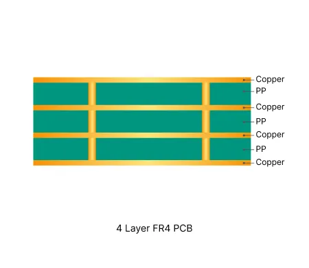
4 Layer FR4 PCB Production Record #FR4-20260505-078
| Parameter | Value | Parameter | Value |
|---|---|---|---|
| PCB Type | FR4 PCB | Quantity | 100 pcs |
| Layers | 4 Layers | Board Type | Panel PCB |
| Dimensions | 119 x 210 mm | Copper Weight | 1oz |
| Thickness | 1.6 mm | Min Track / Spacing | 5/5mil |
| Surface Finish | OSP | Min Hole Size | 0.3mm↑ |
| Solder Mask | Green | Silkscreen | None |
| Stack-up | Default | Impedance Control | No |
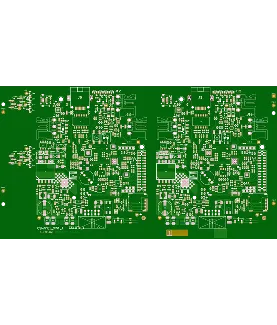
This 4-layer FR-4 order consisted of 200 pieces (100 sets) on 119 × 210 mm boards using 1.6 mm KB-6165F TG150 material with 1 oz copper on both sides. Production used a 1×2 panelization layout, 0.3 mm minimum holes, 5 mil trace/space, and OSP surface finish. The tight 2-day delivery schedule required immediate DFM validation and efficient processing on standard FR-4 flows with 100% flying probe testing.
CAM review identified several file conflicts that were resolved prior to production. Via tenting specifications showed partial open windows versus full cover requirements in the system order; routing layer discrepancies between GM2 and GM3 were standardized to GM3; and drill-to-GM2 size mismatches were aligned to the primary fabrication data. V-CUT positioning presented the highest risk, with multiple pads positioned too close to the panel edge, which could result in copper exposure or breakout during depanelization. These were addressed through targeted adjustments to maintain both electrical integrity and mechanical edge quality. Stamp hole spacing issues were corrected by removing one instance per group to ensure reliable web connections during routing.
All modifications followed confirmed customer approvals and were implemented with full documentation. The via tenting and V-CUT clearance adjustments proved particularly effective in preventing common assembly defects on this panelized layout. Final boards passed electrical testing without issues, maintaining consistent registration and solder mask alignment throughout the urgent run. Completed panels were delivered on schedule to support the customer's timeline.
Standard multilayer solution offering practical routing density and controlled impedance for industrial and consumer electronics.

In-depth guide to the most frequent Engineering Queries (EQ) and DFM issues in Multilayer FR4 PCB (4/6/8+ layers) production. Real factory insights on stack-up confirmation, impedance control, copper balance, inner layer design, via treatment, registration, and practical prevention strategies.
| Order ID | PCB Type | Layers | Dimensions | Solder Mask | Surface Finish | Quantity | Action |
|---|---|---|---|---|---|---|---|
| FR4-20260427-053 | FR4 PCB | 4 | 96.1 x 187 | Green | ENIG (Immersion Gold) | 125 | View detail |
| FR4-20260422-074 | FR4 PCB | 4 | 210 x 100 | Green | OSP | 10 | View detail |
| FR4-20260420-121 | FR4 PCB | 4 | 65.02 x 287.27 | White | HASL with Lead | 5 | View detail |


