PCB Specifications
| Parameter | Value | Parameter | Value |
|---|---|---|---|
| PCB Type | FR4 PCB | Quantity | 20 pcs |
| Layers | 2 Layers | Board Type | Panel PCB |
| Dimensions | 378 x 258 mm | Copper Weight | 1oz |
| Thickness | 1.6 mm | Min Track / Spacing | 6/6mil↑ |
| Surface Finish | OSP | Min Hole Size | 0.2mm |
| Solder Mask | White | Silkscreen | Black |
| Stack-up | Custom | Impedance Control | No |
Manufacturing Timeline
Logistics Information
Key Manufacturing Processes
Manufacturing Summary
This 2-layer FR-4 board measured 378 × 258 mm with 1.6 mm thickness, TG150 material, and 1 oz copper on both sides. Produced as 1800 pieces in 6×15 panels for 20 sets, the order used OSP surface finish, cold white solder mask, and black silkscreen. Line/space remained at standard 6 mil with 0.2 mm minimum holes, and the 12-day schedule included 100% flying probe testing together with routing separation on the high-density panel layout.
DFM review resolved several attribute and panel details. Multiple holes were defined as plated through-hole yet showed undersized or missing pads with no electrical connection in the Gerber data, requiring confirmation of plating intent. Board thickness values appeared inconsistent and were aligned to the nominal 1.6 mm specification. The customer panel drawing lacked routing clearance, so a standard 2 mm slot was proposed and confirmed. Stamp-hole-only data conflicted with the PDF that showed routing slots; the 2.0 mm slots were added after verification. Via treatment also differed between system-required tenting and equal-size openings in the files.
Confirmed hole attributes, panel clearances, and via mask settings were implemented prior to production. The high-volume run achieved consistent OSP surface finish consistency across the dense panels within the planned timeline. Full electrical test reports and quality certificates accompanied the shipment, confirming the boards met the specified mechanical and electrical requirements.
Explore More PCB Manufacturing Resources
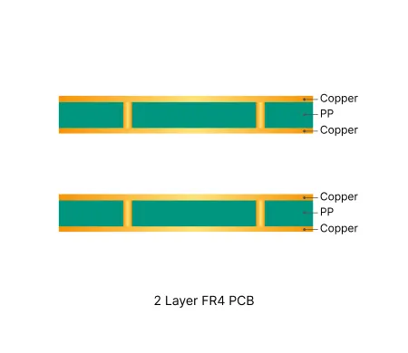
2 Layer FR4 PCB Manufacturing Insights
Discover how AIVON manufactures 2 Layer FR4 PCBs, including double-sided circuit structures, reliable through-hole fabrication processes, manufacturing challenges, and real production experience from customer orders.
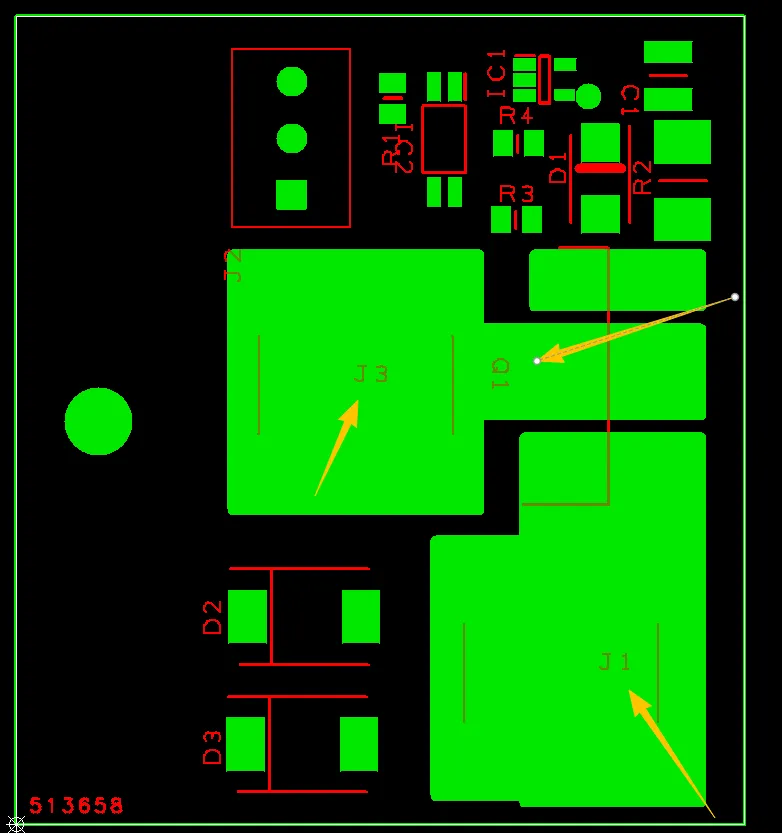
Common Engineering Queries in 2 Layer FR4 PCB Design and Manufacturing
Real Engineering Queries (EQ) and DFM issues for 2 Layer FR4 PCB (double-sided boards) from actual production reviews. Learn how to avoid common problems with via treatment, silkscreen on pads, solder mask openings, hole attributes, board edge clearance, and other frequent design pitfalls.
Real Production Records
| Order ID | PCB Type | Layers | Dimensions | Solder Mask | Surface Finish | Quantity | Action |
|---|---|---|---|---|---|---|---|
| FR4-20260708-079 | FR4 PCB | 2 | 323.77 x 379.03 | White | HASL Lead Free | 400 | View detail |
| FR4-20260708-015 | FR4 PCB | 2 | 15 x 41.7 | White | HASL Lead Free | 5 | View detail |
| FR4-20260630-014 | FR4 PCB | 2 | 126 x 145 | Green | ENIG (Immersion Gold) | 10 | View detail |


