










PCB Specifications
| Parameter | Value | Parameter | Value |
|---|---|---|---|
| PCB Type | FR4 PCB | Quantity | 10 pcs |
| Layers | 2 Layers | Board Type | Panel PCB |
| Dimensions | 126 x 145 mm | Copper Weight | 1oz |
| Thickness | 1.6 mm | Min Track / Spacing | 5/5mil |
| Surface Finish | ENIG (Immersion Gold) | Min Hole Size | 0.3mm↑ |
| Solder Mask | Green | Silkscreen | White |
| Stack-up | Custom | Impedance Control | No |
Manufacturing Timeline
Logistics Information
Key Manufacturing Processes
Manufacturing Summary
This small-batch 2-layer FR-4 board (126 × 145 mm, 1.6 mm thick, TG150, 1 oz copper) was panelized 2×1 for 10 pieces total. The design used 5 mil line/space, immersion gold finish, green solder mask, and white silkscreen. Resin plugging was specified for vias, with 100% flying probe testing required. Process edges of 10 mm were added left and right, and mechanical forming completed the outline with V-cut + routing separation.
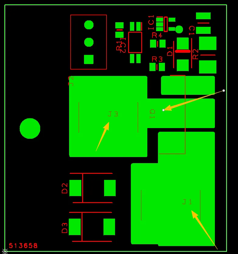
Extensive DFM coordination resolved several layout conflicts. Solder mask openings did not initially match copper features around IC pins and tight-pitch components, risking ink intrusion into PTH pads or broken solder mask bridges. Overlapping silkscreen and mask elements, mismatched outer dimensions in .gko layers, and fiducial/marking placements (including UL and E489133 logos) needed verification. Antenna areas were confirmed for solid copper pour, specific holes for plugged vias versus open mask, and stamp hole additions were aligned. Tight pad-to-hole clearances were adjusted to maintain both trace spacing and solder mask integrity.
All engineering questions were confirmed before release, enabling clean execution of the resin-plugged vias and precise gold plating. The limited 10-piece run was completed within the 11-day schedule, with full electrical test reports, quality certificates, and cross-section analysis delivered. Final boards satisfied the customer’s documentation and assembly requirements.
Explore More PCB Manufacturing Resources
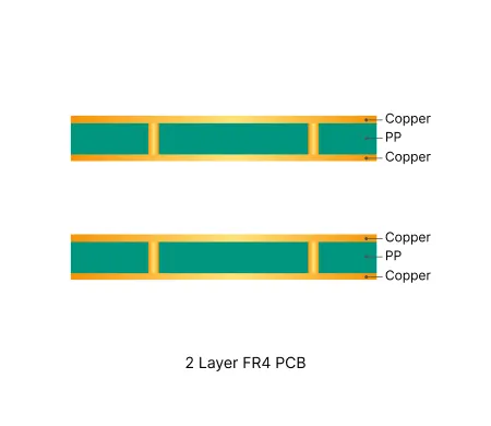
2 Layer FR4 PCB Manufacturing Insights
2 layer FR4 PCBs deliver cost-effective solutions for most electronic designs. Their simple structure enables consistent quality and efficient production cycles.
Common Engineering Queries in 2 Layer FR4 PCB Design and Manufacturing
Real Engineering Queries (EQ) and DFM issues for 2 Layer FR4 PCB (double-sided boards) from actual production reviews. Learn how to avoid common problems with via treatment, silkscreen on pads, solder mask openings, hole attributes, board edge clearance, and other frequent design pitfalls.
Real Production Records
| Order ID | PCB Type | Layers | Dimensions | Solder Mask | Surface Finish | Quantity | Action |
|---|---|---|---|---|---|---|---|
| FR4-20261007-048 | FR4 PCB | 2 | 99.04 x 75.87 | Matte Black | HASL Lead Free | 15 | View detail |
| FR4-20261007-047 | FR4 PCB | 2 | 92.84 x 72.52 | Green | HASL Lead Free | 5 | View detail |
| FR4-20261007-046 | FR4 PCB | 2 | 65 x 97 | Green | HASL Lead Free | 5 | View detail |


