


PCB Specifications
| Parameter | Value | Parameter | Value |
|---|---|---|---|
| PCB Type | FR4 PCB | Quantity | 400 pcs |
| Layers | 2 Layers | Board Type | Panel PCB |
| Dimensions | 323.77 x 379.03 mm | Copper Weight | 2oz |
| Thickness | 1.6 mm | Min Track / Spacing | 6/6mil↑ |
| Surface Finish | HASL Lead Free | Min Hole Size | 0.3mm↑ |
| Solder Mask | White | Silkscreen | Black |
| Stack-up | Custom | Impedance Control | No |
Manufacturing Timeline
Logistics Information
Key Manufacturing Processes
Manufacturing Summary
This 2-layer FR-4 board measured 323.77 × 379.03 mm with 1.6 mm thickness, TG150 material, and asymmetric copper of 1 oz inner / 2 oz outer. Produced in high volume as 6400 pieces across 8×2 panels for 400 sets, the order used lead-free HASL surface finish, cold white solder mask, and black silkscreen. Line/space remained at standard 6 mil with 0.3 mm minimum holes, and the 3-day schedule included engineering test fixtures together with routing separation.
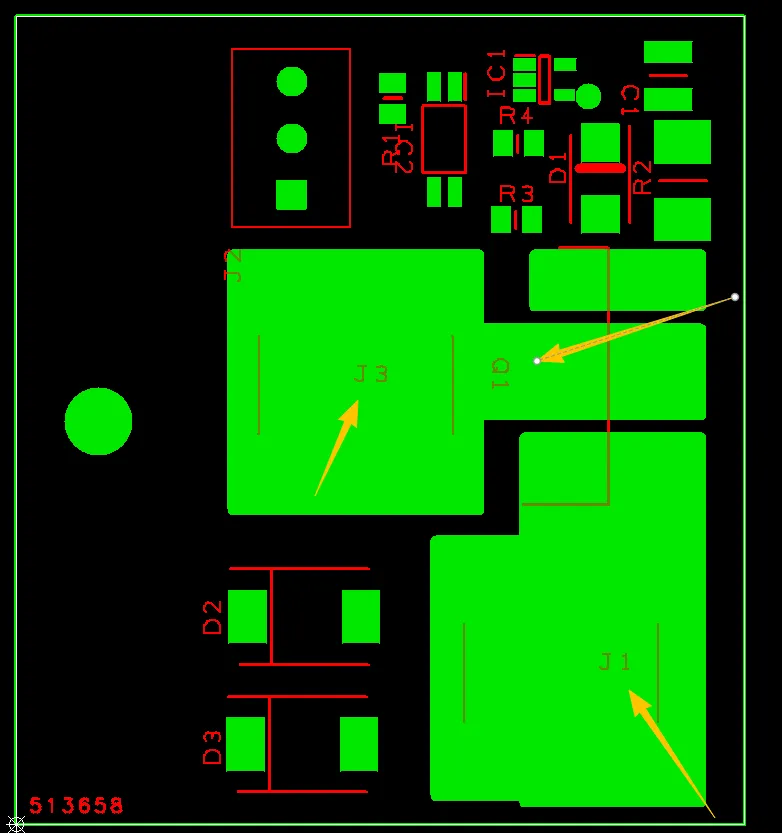
DFM coordination resolved several layout and process details. Via treatments varied between full openings, small windows, and the system-required tenting; the final mask approach was confirmed. Rectangular features on the keepout layer overlapping traces were reviewed for omission. Connection tabs lacked mouse bites, so standard additions were evaluated to aid depanelization. Small white-marked characters risked reduced legibility after processing, and 0.3 mm vias were proposed without compensation to maintain strict original window sizes. Pad geometries showing potential tombstone risk were adjusted for uniform SMT pad sizing.
Confirmed via mask, tab, and pad modifications were implemented prior to production. The high-volume run achieved consistent lead-free HASL coverage on the heavier copper side within the accelerated timeline. Full electrical test reports and quality certificates accompanied the shipment, confirming the boards met the specified mechanical and electrical requirements.
Explore More PCB Manufacturing Resources
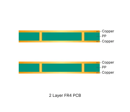
2 Layer FR4 PCB Manufacturing Insights
Discover how AIVON manufactures 2 Layer FR4 PCBs, including double-sided circuit structures, reliable through-hole fabrication processes, manufacturing challenges, and real production experience from customer orders.
Common Engineering Queries in 2 Layer FR4 PCB Design and Manufacturing
Real Engineering Queries (EQ) and DFM issues for 2 Layer FR4 PCB (double-sided boards) from actual production reviews. Learn how to avoid common problems with via treatment, silkscreen on pads, solder mask openings, hole attributes, board edge clearance, and other frequent design pitfalls.
Real Production Records
| Order ID | PCB Type | Layers | Dimensions | Solder Mask | Surface Finish | Quantity | Action |
|---|---|---|---|---|---|---|---|
| FR4-20261009-004 | FR4 PCB | 1 | 58.85 x 65.86 | Green | HASL Lead Free | 50 | View detail |
| FR4-20261007-048 | FR4 PCB | 2 | 99.04 x 75.87 | Matte Black | HASL Lead Free | 15 | View detail |
| FR4-20261007-047 | FR4 PCB | 2 | 92.84 x 72.52 | Green | HASL Lead Free | 5 | View detail |


