Introduction
This engineering case study examines a 12-layer high-reliability FR-4 PCB order with TG170 material, 1.6mm finished thickness, and ENIG surface finish(#FR4-20260430-032). Such multilayer boards are common in industrial control and computing applications but frequently trigger detailed CAM engineering review due to complex stackup requirements, tight feature tolerances, and panelization specifications.
During the standard DFM analysis, our CAM team identified several manufacturability concerns related to solder mask definition, copper clearance near V-CUT areas, stackup compatibility with production capabilities, and fabrication note consistency. These issues are typical for 12-layer designs where customer intent must be carefully balanced against actual fabrication process windows. Early clarification prevents production delays, yield loss, and potential field failures.
This case demonstrates why thorough engineering questions (EQs) are raised before releasing Gerber data to production and how proactive adjustments ensure reliable manufacturing outcomes.
Order Overview
The project involves a 12-layer PCB using FR-4 TG170 base material, sized at 165.1mm × 215.58mm, with 1oz copper on both outer layers and standard inner layer weights. Finished board thickness is specified at 1.6mm. The design calls for ENIG surface finish, white solder mask on both top and bottom, and 100% flying probe testing. Minimum hole size is 0.3mm, with V-CUT panelization in a 1x1 configuration plus 4mm process edges on top and bottom.
Quantity is 20 panels (20 sets). The stackup includes blind vias and requires careful impedance control considerations, although not explicitly documented in all layers. Production was planned with mechanical forming and standard etching processes. These parameters place the board in a medium-to-high complexity category for multilayer fabrication, particularly regarding registration, copper balance, and solder mask registration tolerances.
Main Engineering Questions Found During CAM Review
Stackup Adjustment Requirement
After reviewing the customer-provided stackup, our CAM engineer identified inconsistencies with our standard 12-layer process capabilities for TG170 material at 1.6mm finished thickness. We noticed the proposed dielectric thicknesses and copper distribution would risk copper imbalance and potential warpage during lamination.
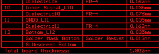
Figure 1: Customer-provided stackup
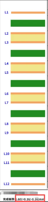
Figure 2: Adjusted stackup of 1.6mm finished thickness
We suggested a minor adjustment to the layer stackup to better align with proven production parameters while maintaining the overall impedance profile and signal integrity targets. According to IPC-2221 guidelines for multilayer construction, such adjustments are common to ensure symmetrical copper distribution and controlled resin flow.
If ignored, the original stackup could lead to board warpage exceeding acceptable limits, delamination at high-Tg interfaces, or via cracking during thermal cycling. Our engineering team confirmed the revised stackup with the customer before proceeding to avoid these risks.
Solder Mask Clearance and Opening Issues
Several solder mask related concerns were flagged. First, the provided artwork showed solder mask openings on certain traces measuring only 3mil square. Our process capability review determined these fine openings could not be reliably produced without risking incomplete development or ink residue.
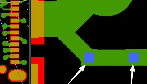
Figure 3: Solder mask openings of only 3mil square
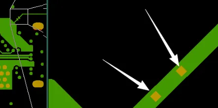
Figure 4: The other 3mil square openings
Our engineer suggested deleting these two 3mil square openings on the traces. We noticed that attempting such small features would likely result in solder mask encroaching on the copper, leading to poor solderability or potential opens during assembly.
Additionally, some pad openings appeared smaller than the finished pads, which could leave solder mask on pad edges. If not clarified, this would cause solderability issues, weak joints, or assembly failures. Per IPC-A-600 acceptability criteria, consistent solder mask to pad clearance is critical for reliable SMT assembly.
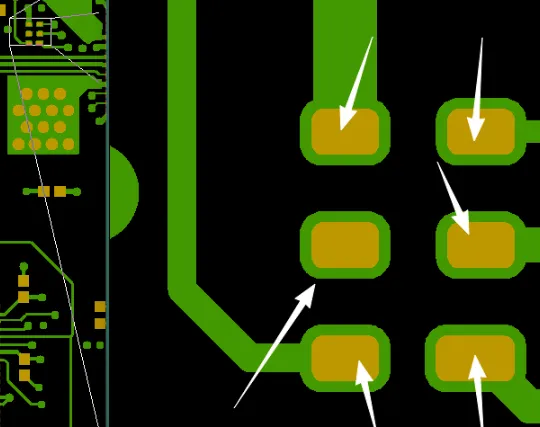
Figure 5: Some pad openings appeared smaller than the finished pads.
Board Thickness and Fabrication Note Consistency
The order parameters listed 1.6mm finished thickness, but cross-checking with the fabrication drawing revealed minor discrepancies in tolerance interpretation. Our team asked for confirmation on the exact finished board thickness to follow, as this directly impacts impedance calculations, mechanical fit, and overall stackup planning.
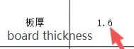
Figure 6: Standard 1.6mm finished thickness
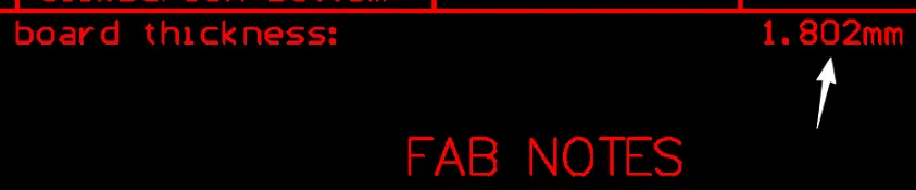
Figure 7: Customer-provided 1.802mm board thickness
Inconsistent notes between Gerber files and drawings are a frequent trigger for EQs. Proceeding without alignment could result in boards falling outside customer mechanical specifications, leading to assembly rejection or field reliability concerns.
Panelization and Process Edge Verification
The customer requested V-CUT panelization. We provided our standard panel layout with 4mm process edges top and bottom, including fiducials and tooling holes. Confirmation was required to ensure the layout matched customer expectations for depanelization and downstream assembly.
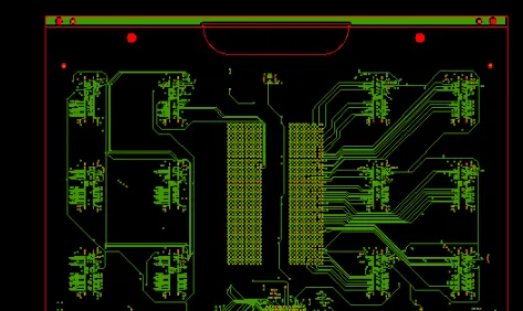
Figure 8: Standard panel layout
Our engineer confirmed the copper clearance near V-CUT lines. We noticed some copper features were too close to the scoring area. If left unadjusted, depanelization could expose copper edges, increasing the risk of short circuits during handling or conformal coating application.
Silkscreen and UL Marking Requirements
The customer requested specific UL marking and date code placement on the top silkscreen layer. We confirmed the exact positioning and format to ensure compliance without interfering with component placement or readability.
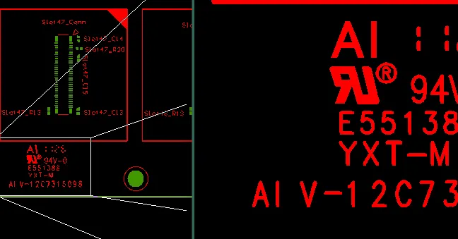
Figure 9: Requested specific UL marking
Inconsistent Solder Mask Color Requirements
We noticed a clear mismatch between the order system (specifying white solder mask on both top and bottom) and the actual design files. Our engineer flagged this inconsistency immediately because solder mask color directly affects ink type selection, exposure parameters, and final appearance.

Figure 10: Solder mask color request
If left unresolved, mismatched color settings could lead to incorrect mask application, color deviation in the finished boards, or even production using the wrong ink formulation, resulting in poor adhesion or cosmetic defects that fail customer inspection. We asked the customer to confirm the final solder mask color requirement before proceeding.
Suggested EQ Categories
Stackup & Material Issues
- Stackup optimization for 12-layer TG170 construction
- Finished thickness confirmation
Solder Mask & Silkscreen Issues
- Minimum solder mask opening limitations
- Pad encroachment risk
- UL/date code placement
Panelization & Process Optimization
- V-CUT clearance verification
- Process edge and fiducial confirmation
File & Manufacturing Data Issues
- Production file confirmation
- Fabrication note alignment
Manufacturing Risks and DFM Insights
This case highlights several recurring DFM challenges in multilayer PCBs. Tight solder mask openings are a common customer oversight — designers often assume photoimageable solder mask can resolve features at the same scale as copper. In reality, for white solder mask on dense 12-layer boards, maintaining 4-5mil minimum reliable openings is safer to prevent ink bridging or residue.
Stackup mismatches frequently cause the most significant delays. Without early adjustment, copper imbalance can lead to excessive bow and twist, violating IPC-6012 Class 2 or 3 requirements and causing assembly problems. V-CUT proximity to copper is another critical area — post-depanelization edge shorts or cosmetic defects are expensive to rework.
If these EQs had been ignored, potential outcomes included high scrap rates from warpage, via reliability failures under thermal stress, solder mask related assembly defects, and multiple production revision cycles. These issues not only increase costs but can damage customer confidence in the supply chain.
How the Engineering Team Resolved the Issues
Our CAM team prepared updated production files incorporating the agreed stackup modifications, removed the problematic 3mil openings, and adjusted clearances around V-CUT lines. We provided the revised Gerber/ODB++ package along with a detailed comparison of changes.
After customer confirmation on all points — including panel layout, thickness, and marking — the job was released for production. This collaborative approach minimized risk and ensured first-pass success.
“We always prefer to confirm these details upfront,” noted our senior CAM engineer. “Adjusting copper near scoring areas or fine-tuning dielectric spacing early prevents far more costly issues downstream.”
Final Manufacturing Outcome
All engineering questions were resolved through clear communication and data updates. The revised production files were approved by the customer, and the order was successfully released to the production floor with optimized parameters for yield and reliability. The 20 panels are proceeding under standard process controls with full electrical testing.
Key Takeaways for PCB Designers
- Provide complete and consistent stackup documentation, including dielectric materials and target thicknesses, early in the quoting process.
- Respect minimum solder mask feature sizes — consult with your fabricator before using sub-4mil openings, especially with white ink.
- Ensure adequate copper clearance (typically 0.5mm or more) from V-CUT or scoring lines to prevent edge exposure.
- Align all fabrication notes between drawings, README files, and Gerber layers to avoid conflicting requirements.
- Define hole attributes clearly (plated vs non-plated, via types) and include any impedance requirements with target layers and tolerances.
- For multilayer boards, consider copper balance across layers to minimize warpage risk.
- Request panelization drawings for approval when using V-CUT or tab-routing to confirm fiducials and process edges.
- Maintain open communication during the CAM review phase — quick responses to EQs significantly reduce lead time.
FAQ
Q1: Why is stackup adjustment often required for multilayer PCBs?
A1: Fabricators optimize stackups based on available core and prepreg materials, press capabilities, and copper balance for the specific layer count and thickness. Adjustments ensure reliable lamination, controlled impedance, and minimal warpage while staying within IPC-6012 standards.
Q2: What problems can tiny solder mask openings cause?
A2: Openings smaller than process capability (such as 3mil squares) often result in incomplete mask removal, ink on pads, or bridging. This leads to poor solder wetting, tombstoning, or assembly defects. Manufacturers typically recommend minimum reliable feature sizes for the chosen mask color and technology.
Q3: Why check copper clearance near V-CUT lines?
A3: During depanelization, scoring can expose or damage copper too close to the edge. This creates shorting risks, cosmetic defects, or reliability issues in the final assembly. Proper clearance protects the functional circuitry.
Q4: How important is finished board thickness confirmation?
A4: Thickness directly affects mechanical fit, impedance, and component assembly. Discrepancies between drawing and data can cause boards to be rejected at incoming inspection or fail in application.
Q5: What is the benefit of early EQ communication in PCB production?
A5: It prevents costly scrap, reduces lead time, and ensures the final product meets both design intent and manufacturing realities. Most issues can be resolved with small data adjustments before lamination begins.
Q6: Should designers always provide panelization drawings?
A6: For V-CUT or custom panelization, yes. Confirming the layout with the factory avoids misalignment of fiducials, tooling holes, or process edges that could complicate SMT processing.