8-layer PCBs with 1oz copper and tight feature spacing frequently challenge manufacturing tolerances during CAM review. This case reviews order, a compact 138.43 × 136.9 mm board built on TG170 FR-4 material. During our standard engineering analysis, several critical DFM issues emerged that required customer clarification before production release.
As a senior CAM engineer with extensive experience in multilayer fabrication, I always emphasize thorough file verification. In this instance, minimum clearance violations, resin plug inconsistencies, and outline layer mismatches stood out as primary concerns. Our team raised targeted Engineering Questions (EQs) to align the production data with factory capabilities and prevent downstream defects.
Order Overview
This 8-layer FR-4 board ( #FR4-20260430-009 ) featured TG170 base material, 1.6mm finished thickness, and 1oz copper on both inner and outer layers. The design specified ENIG surface finish, 0.2mm minimum hole size, green solder mask on both sides, and white silkscreen. Production involved 100% flying probe testing, mechanical forming, and resin plugged holes as a key requirement. The panel was a single-piece 1×1 configuration with no process edges specified and a quantity of 20 pieces.
Customer files included multiple versions, necessitating confirmation of the primary manufacturing dataset. Special notes highlighted resin hole plugging and potential press-fit holes, requiring careful verification against the provided Gerber and ODB data.
Main Engineering Questions Found During CAM Review
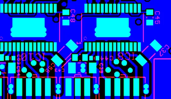
1. Critical Hole-to-Line Clearance Violation on 8-Layer Board
The most significant issue identified was a hole-to-line spacing of only 4mil in multiple locations on this 8-layer construction. For standard 8-layer processing with 1oz copper, our manufacturing guidelines typically require a minimum of 6mil to ensure reliable etching and registration across all layers.

Figure 1: a hole-to-line spacing of only 4mil in multiple locations
We noticed this tight clearance immediately during DFM analysis. Our CAM engineer flagged it because insufficient spacing risks copper bridging or incomplete etching, especially in multilayer boards where inner layer registration tolerances accumulate. We requested customer optimization of the affected areas to bring spacing within acceptable limits.
If this EQ had been ignored and production proceeded, the result could have been short circuits between vias and traces, copper residues causing intermittent failures, or severe yield loss after etching. In extreme cases, this leads to scrap boards and costly delays. According to IPC-2221 spacing recommendations, the original 4mil approached the lower manufacturability limit for this layer count and copper weight.
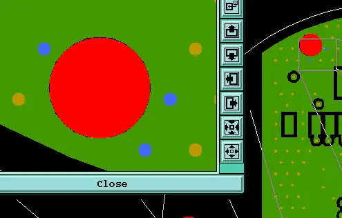
2. Resin Plugged Holes vs. Actual Solder Mask Openings
Another key confirmation point involved resin plugging requirements. The customer specified resin plugged holes, yet portions of the provided data showed solder mask openings on those same holes, creating a direct conflict.
Figure 2: resin plugged holes and solder mask openings on the same holes
Our engineering team identified this inconsistency after cross-checking the drill files against the plugging notes. We asked for explicit confirmation on which holes required full plugging versus those intended for standard via treatment. This step is crucial because mismatched plugging can affect flatness, solderability, and long-term reliability.
Proceeding without clarification risked resin voids, incomplete plugging leading to solder wicking into vias during assembly, or poor planarity causing assembly failures. We have seen such mismatches result in delamination or cosmetic defects that fail final inspection.
3. Outline Layer Mismatch and Multiple File Versions
The GM and GM15 outline layers showed inconsistencies in dimensions and features. Additionally, the customer provided multiple file sets, prompting us to confirm the authoritative production dataset.
Figure 3: outline layers showed inconsistencies in dimensions and features
We noticed these discrepancies during initial file loading and raised an EQ to avoid using conflicting data that could lead to incorrect board outlines or misalignment during routing. Our team requested the customer to specify the primary file for all subsequent processing.
Without resolution, this could cause dimensional errors, misaligned tooling holes, or boards failing mechanical specifications, leading to scrap or rework.
4. Press-Fit Hole and Production File Confirmation
We also received customer notes indicating the presence of press-fit holes, but the actual drill files and fabrication notes required explicit verification. Our CAM team identified that some holes appeared designated for press-fit applications based on size and location, yet the provided data lacked clear attributes or tolerances specific to press-fit processing.
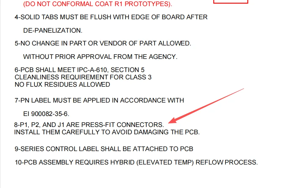
Figure 4: customer notes indicating the presence of press-fit holes
After reviewing the stackup and drill information, we raised an EQ asking the customer to confirm whether these holes truly required press-fit treatment, including any special tolerances, plating requirements, or back-drill considerations. We noticed potential ambiguity in the hole attributes that could affect final mechanical fit during connector assembly.
If left unconfirmed, proceeding with standard via processing on press-fit designated holes could result in insufficient hole wall strength, poor connector retention, or dimensional mismatch during assembly, leading to field failures such as loose connections or signal instability. Conversely, applying unnecessary press-fit parameters to standard holes might cause plating issues or increased cost without benefit. This confirmation ensured our production files accurately reflected the intended mechanical requirements.
Suggested EQ Categories
File & Manufacturing Data Issues
- Multiple conflicting file versions and outline mismatches (GM/GM15)
- Which file to use as the primary manufacturing reference
Hole & Tolerance Issues
- Hole-to-line clearance below 6mil minimum on 8-layer board
- Press-fit hole requirements
Special Structure Clarification
- Resin plugged hole requirements vs. actual data openings
- Inconsistent plugging specifications
Manufacturing Risks and DFM Insights
This case underscores common challenges in 8-layer designs: designers often push clearance limits without accounting for multilayer etching and registration tolerances. The 4mil spacing was a clear DFM red flag that could have caused etching residuals or shorts if not addressed.
Resin plugging conflicts are another frequent trigger. If ignored, incomplete or mismatched plugging can lead to via contamination, solder wicking, or board warpage during reflow. File version mismatches further compound risks by introducing dimensional errors that only surface after lamination and routing.
Such issues typically cause production delays, multiple review cycles, increased engineering time, and potential yield reduction if not caught early.
How the Engineering Team Resolved the Issues
Our team coordinated directly with the customer, providing annotated screenshots highlighting the tight clearance areas and layer conflicts. For the clearance violation, we recommended widening the affected spaces or adjusting via positions where possible. On resin plugging, we confirmed the specific holes requiring fill and updated mask data accordingly.
After receiving confirmation on the primary file set, we reconciled the outline layers and prepared a unified production package. We noticed the outline mismatch early and adjusted our CAM files to maintain dimensional accuracy. This proactive approach reduced manufacturing risk and protected overall yield.
Final Manufacturing Outcome
All EQ points received clear customer confirmation. Clearance optimizations were implemented where feasible, resin plugging parameters were aligned, and the authoritative production files were approved. The order was successfully released for fabrication with updated manufacturing data.
Key Takeaways for PCB Designers
- Maintain minimum 6mil hole-to-line clearance on 8-layer boards with 1oz copper to ensure reliable etching and avoid DFM flags.
- Ensure solder mask data fully matches resin plugging requirements — avoid openings on holes designated for plugging.
- Use consistent layer naming and provide a single authoritative Gerber/ODB package to prevent version conflicts.
- Clearly document special structures like press-fit holes and plugging in fabrication notes with supporting drawings.
- Verify outline layers (e.g., GM/GM15) across all files before submission to eliminate dimensional discrepancies.
- Account for multilayer registration tolerances when setting tight features in high-layer-count designs.
- Respond to EQs with specific file updates rather than vague approvals to streamline production release.
- Perform internal DFM checks against common factory capabilities before sending files for quotation.
FAQ
Q1: Why is 4mil hole-to-line spacing problematic on an 8-layer PCB?
A1: At higher layer counts, etching tolerances and inner layer registration make tight clearances prone to shorts, residuals, or open circuits. Factories typically require 6mil+ for reliable yields per standard DFM guidelines.
Q2: What happens if resin plugged hole data conflicts with solder mask openings?
A2: It can cause incomplete plugging, resin voids, solder wicking into vias, or planarity issues during assembly, potentially leading to reliability failures or cosmetic defects.
Q3: Why do CAM engineers request confirmation on multiple file versions?
A3: Conflicting files (e.g., different outlines or features) risk manufacturing the wrong board version. Clear selection of the primary dataset prevents dimensional errors and production mistakes.
Q4: How can designers avoid outline layer mismatches?
A4: Ensure all mechanical/outline layers are identical across the full Gerber set and include a clear fabrication drawing referencing the correct layers.
Q5: What is the risk of ignoring clearance EQs in multilayer boards?
A5: High risk of short circuits, etching defects, reduced yield, and potential field failures due to compromised trace isolation under manufacturing variations.