In PCB fabrication, even compact boards with standard specifications can present significant manufacturability challenges during engineering review. This case examines a 6-layer FR-4 board (#FR4-20260422-027) measuring 30x30mm, ordered in 100pcs (25 sets). During our CAM review, several critical issues emerged that required clarification with the customer to prevent production defects.
As a senior CAM engineer with over 15 years in the industry, I have seen how small oversights in design data can lead to major issues in etching, plating, solder mask application, and final assembly. This article details the real engineering questions (EQs) raised, the manufacturing risks involved, and the resolutions implemented before releasing the job to production.
Order Overview
This was a standard 6-layer rigid PCB using FR-4 material with TG150. The board thickness was specified at 1.6mm, with copper weights of 0.5oz inner layers and 1oz outer layers. Surface finish was ENIG (immersion gold), and the design included 0.2mm minimum hole size with 100% flying probe testing. Panelization was 2x2 with routing and 4mm process edges. Special requirements included resin plugging for certain vias and mechanical forming.
While the overall parameters appeared routine, the combination of tight feature spacing on outer layers, via plugging requirements, and minor inconsistencies between layers triggered a thorough DFM review. Our CAM team processes hundreds of similar jobs monthly, and this one highlighted classic gaps between design intent and production capability.
Main Engineering Questions Found During CAM Review
1. Insufficient Solder Mask Bridge Clearance on Outer Layers
We noticed that several areas on the outer layers had pad-to-pad or pad-to-trace spacing of only 5.5-6mil. After applying our standard solder mask compensation for 1oz copper and green solder mask, the remaining bridge width fell below our reliable manufacturing threshold. Our standard requires a minimum 7.5mil original spacing to guarantee a solid solder mask bridge.
Figure 1: Pad-to-pad or pad-to-trace spacing of only 5.5-6mil
Our engineer suggested adjusting the copper clearance because we noticed the tight spacing would likely result in incomplete mask coverage or bridging after processing. If ignored, this could lead to solder mask voids, exposed copper, or short circuits during assembly. In worst cases, it causes solder bridging during SMT, leading to assembly failures and costly rework or scrap boards.
According to typical IPC-A-600 acceptability criteria, such narrow bridges increase defect risk, especially on ENIG-finished boards where solderability is critical. We requested customer confirmation to either widen clearances or accept potential cosmetic and functional risks.
2. Conflict Between Resin Via Plugging and Solder Mask Openings
The fabrication notes required resin plugging for specific vias. However, the Gerber files showed single-side solder mask openings on some of these same vias. This mismatch creates a serious process conflict: plugged vias should typically have full solder mask coverage or defined tenting, not open windows.

Figure 2: Single-side solder mask openings on some of these same vias
We identified this during stackup and drill program verification. If production proceeded without clarification, the plugging process could push resin into mask openings or cause inconsistent surface flatness, leading to poor solderability, via cracking under thermal stress, or plating voids. Our CAM team has seen such conflicts result in delamination or open circuits after reflow.
3. Via Proximity to NPTH Holes and Dimension Inconsistencies
Several plated vias were positioned too close to non-plated through holes (NPTH). We recommended shifting them to maintain at least 0.3mm spacing where routing allowed.
Figure 3: Plated vias are too close to non-plated through holes (NPTH) in the gerber file.
Additionally, we found a dimension mismatch: the "boardedge rout" layer showed 29.25mm x 29.25mm while the outer layer indicated 30mm x 30mm. Our team confirmed we would fabricate to the 30x30mm outline as per the primary fabrication data.
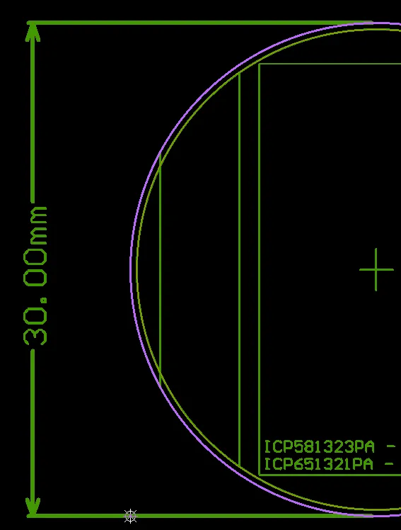
Figure 4: Mismatch between "boardedge rout" layer and the outer layer
Tight via-to-hole spacing risks drill wander, breakout, or insufficient dielectric during routing, potentially causing short circuits or weakened board integrity after depanelization. If not addressed, exposed copper at edges or via damage could occur, violating IPC-6012 Class 2 requirements for hole registration and edge clearance.
4. Silkscreen Placement Issues and Stackup Clarification
Parts of the silkscreen legend overlapped pads or were positioned too close, which can interfere with soldering.
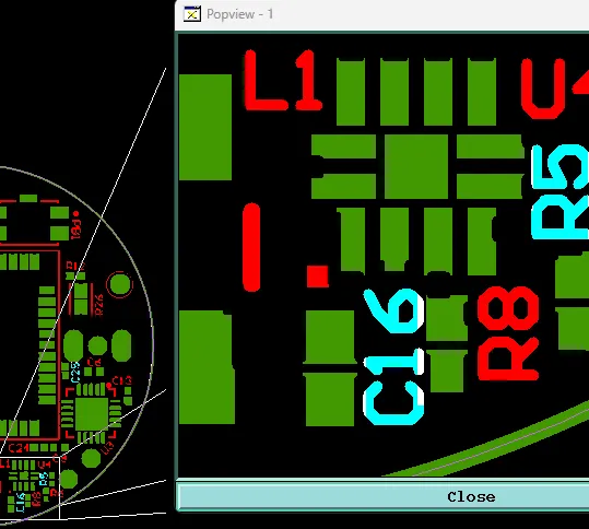
Figure 5: The silkscreen legend overlapped pads or are positioned too close.
We also needed confirmation on the press stackup. The customer referenced a previous version using 7628 PP, but due to low copper density, we suggested alternative PP sheets to avoid glass weave exposure.
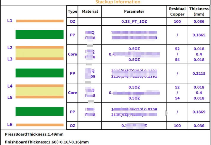
Figure 6: Adjusted press stackup info
Board thickness targets also required final confirmation to ensure consistency.
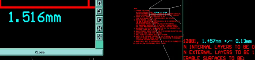
Figure 7: Board thickness requirement mismatch
Our engineer confirmed the panelization drawing and recommended the PP change to maintain better surface quality and reduce warpage risk. Ignoring the silkscreen issue could result in poor component placement or cosmetic defects visible after assembly.
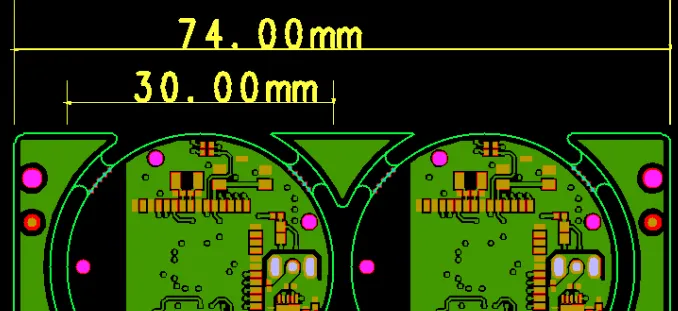
Figure 8: Panelization drawing
Manufacturing Risks and DFM Insights
This case underscores several common DFM pitfalls. Tight solder mask clearances are frequent triggers because designers often work with ideal simulation tools that do not account for real-world mask expansion, alignment tolerances, and copper etching factors. Similarly, via plugging combined with mask definitions requires precise layer alignment in the data set.
If the solder mask bridge issue had been ignored, we could have faced high yield loss from mask-related shorts or opens. The via plugging conflict risked resin overflow or incomplete plugging, leading to potential via reliability failures under thermal cycling. Dimension and spacing problems increase the chance of edge defects and mechanical weakness post-routing.
In our experience, such issues often lead to multiple review cycles, delaying delivery by days or weeks. Early EQ communication prevents scrap and ensures the final boards meet both electrical and mechanical expectations.
How the Engineering Team Resolved the Issues
Our team compiled detailed screenshots highlighting each problem area and sent a comprehensive EQ list to the customer. For the solder mask clearance, we proposed copper adjustments in non-critical areas. The via plugging conflict was resolved by clarifying mask definitions and confirming plug-and-cap requirements.
We adjusted the stackup using alternative PP materials to avoid glass weave print-through while maintaining the target 1.6mm thickness. Panelization and outline dimensions were aligned to the dominant 30x30mm specification. All changes were documented and re-verified in the CAM system before final approval.
After customer confirmation, we optimized the drill program, updated solder mask and legend files, and confirmed the production stackup. This proactive approach minimized risks and kept the job on schedule.
Final Manufacturing Outcome
Following clarification on all points, the engineering data was updated, and the job was approved for production. The panelization, stackup, and critical feature clearances were finalized according to agreed parameters. The order proceeded through inner layer imaging, lamination, drilling, plating, and surface finishing without further major issues.
Key Takeaways for PCB Designers
- Always verify minimum solder mask bridge requirements against your chosen copper weight and mask color. For 1oz green mask, maintain at least 7-8mil spacing in Gerber data before compensation.
- Ensure via plugging specifications match solder mask definitions precisely. Mixed plugged/tented and open vias require clear layer-by-layer instructions.
- Provide consistent board outline dimensions across all layers, particularly between rout layers and copper layers.
- Position silkscreen at least 0.1-0.15mm away from pads to prevent soldering interference.
- Reference stackup details carefully, including PP types, and be open to manufacturer suggestions for low copper density designs to avoid surface defects.
- Include clear hole attributes and tolerances in fabrication notes to reduce ambiguity during CAM review.
- Test your design data with DFM tools that simulate actual manufacturing compensation before submission.
FAQ
Q1: Why is solder mask bridge width so critical in PCB manufacturing?
A1: Insufficient bridge width after compensation can cause mask openings between pads, leading to solder shorts during assembly or exposed copper that oxidizes over time. Factories apply expansion tolerances, so original design spacing must exceed the minimum reliable bridge (typically 7.5mil+ for 1oz).
Q2: What happens if via plugging and solder mask openings conflict?
A2: The processes interfere, potentially causing incomplete plugging, resin on pads, or unreliable via protection. This can result in via cracking, poor thermal performance, or assembly defects. Clarification ensures proper tenting or defined openings.
Q3: Why do factories adjust via positions near NPTH holes?
A3: Close proximity risks drill breakage, registration errors, or dielectric breakdown after routing. Maintaining 0.3mm+ spacing improves reliability and reduces breakout risk, aligning with IPC-6012 standards.
Q4: How important is consistent board outline data across layers?
A4: Inconsistent dimensions can lead to incorrect panelization, routing errors, or final board size deviations. Factories prioritize the primary fabrication layer but require confirmation to avoid dimensional tolerance issues.
Q5: Can PP material choices be changed during engineering review?
A5: Yes, especially for low copper density designs where heavy glass styles like 7628 may cause print-through. Manufacturers recommend alternatives to ensure flatness and cosmetic quality while maintaining thickness and impedance targets.
Q6: What is the benefit of early EQ communication in PCB orders?
A6: It prevents production of defective boards, reduces scrap costs, avoids delays from mid-process rework, and builds better understanding between designer and manufacturer for future jobs.