6 Layer FR4 PCB Production Record #FR4-20260422-027
| Parameter | Value | Parameter | Value |
|---|---|---|---|
| PCB Type | FR4 PCB | Quantity | 100 pcs |
| Layers | 6 Layers | Board Type | Panel PCB |
| Dimensions | 30 x 30 mm | Copper Weight | 1oz |
| Thickness | 1.6 mm | Min Track / Spacing | 6/6mil↑ |
| Surface Finish | ENIG (Immersion Gold) | Min Hole Size | 0.2mm |
| Solder Mask | Blue | Silkscreen | White |
| Stack-up | Default | Impedance Control | No |
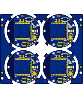
This 6-layer FR-4 PCB order consisted of 100 pcs (25 sets) of compact 30 × 30 mm boards at 1.6 mm finished thickness, using 0.5 oz inner / 1 oz outer copper, 0.2 mm minimum holes, 6 mil trace/space, blue solder mask, white silkscreen, and ENIG surface finish. Production involved 2×2 panelization with mechanical routing, resin plugging of vias, and 100% flying probe testing. The small panel size and 13-day delivery window required tight control over lamination and plating sequences to maintain registration and thickness consistency across the batch.
During CAM review, several DFM issues were identified and resolved. Gerber via-to-NPTH clearances were adjusted to exceed 0.3 mm to prevent drill breakage risk, while board outline dimensions were standardized to 30 × 30 mm after reconciling the routed edge layer (29.25 mm) with the design layers. Solder mask bridge concerns arose on pads with original 5.5–6 mil spacing; after compensation on 1 oz copper, minimum bridge width requirements were confirmed and enforced. Via plugging also required clarification due to single-side solder mask openings in the files. These adjustments, along with lamination PP selection to avoid glass weave exposure, followed established solder mask bridge and via plugging handling from prior 6-layer production.
All engineering changes were documented and approved prior to release. The order completed without deviation in electrical testing or final inspection, with consistent ENIG coverage and reliable resin plug integrity. Boards were delivered on schedule, demonstrating repeatable manufacturing for this compact multilayer configuration.
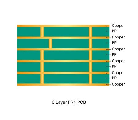
Six layer FR4 boards provide optimized routing density and power distribution. They require precise lamination and plating process control to maintain yield and reliability.

In-depth guide to the most frequent Engineering Queries (EQ) and DFM issues in Multilayer FR4 PCB (4/6/8+ layers) production. Real factory insights on stack-up confirmation, impedance control, copper balance, inner layer design, via treatment, registration, and practical prevention strategies.
| Order ID | PCB Type | Layers | Dimensions | Solder Mask | Surface Finish | Quantity | Action |
|---|---|---|---|---|---|---|---|
| FR4-20260520-046 | FR4 PCB | 2 | 94.21 x 275 | Green | ENIG (Immersion Gold) | 75 | View detail |
| FR4-20260515-068 | FR4 PCB | 14 | 244 x 267 | Green | ENIG (Immersion Gold) | 10 | View detail |
| FR4-20260506-017 | FR4 PCB | 6 | 55 x 41.7 | Green | ENIG (Immersion Gold) | 15 | View detail |


