










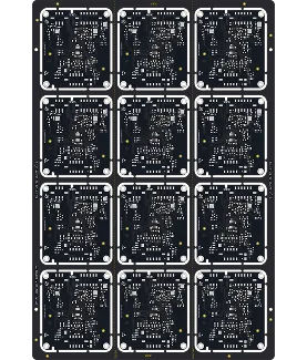
PCB Specifications
| Parameter | Value | Parameter | Value |
|---|---|---|---|
| PCB Type | FR4 PCB | Quantity | 25 pcs |
| Layers | 6 Layers | Board Type | Panel PCB |
| Dimensions | 239 x 355 mm | Copper Weight | 2oz |
| Thickness | 1.6 mm | Min Track / Spacing | 6/6mil↑ |
| Surface Finish | HASL Lead Free | Min Hole Size | 0.3mm↑ |
| Solder Mask | Black | Silkscreen | None |
| Stack-up | Default | Impedance Control | No |
Manufacturing Timeline
Logistics Information
Key Manufacturing Processes
Manufacturing Summary
This 6-layer FR-4 board required careful stackup alignment between customer lamination drawing and standard production configurations. Panelization included V-cut and routing with connection tabs reviewed for stamp hole placement. Small solder mask legend elements were identified as below reliable process capability, while overall layer configuration needed adjustment to match available materials and press parameters for consistent thickness and registration.
DFM review highlighted deviations in the proposed lamination stack that could affect interlayer registration and thermal performance. Connection tabs without stamp holes were confirmed as intentional to maintain panel strength during handling. Tiny solder mask characters risked incomplete or illegible marking. After customer feedback on suggested options, the stackup was revised to a manufacturable configuration using standard prepreg and core combinations that preserved electrical and mechanical properties.
Revised stackup parameters were implemented and verified before full production release. This multilayer PCB stackup adjustment process ensured reliable pressing and avoided potential delamination or thickness variation. The order completed with 100% electrical testing and standard quality documentation, meeting all functional requirements within the agreed delivery timeframe.
Explore More PCB Manufacturing Resources
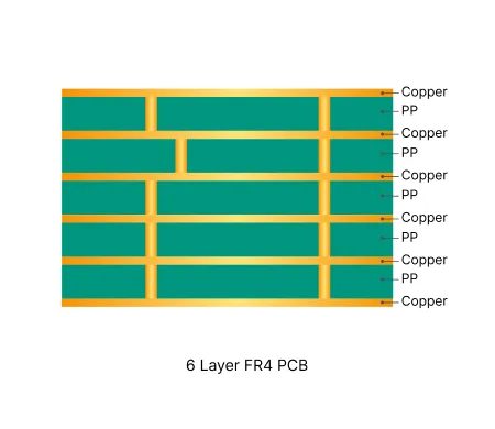
6 Layer FR4 PCB Manufacturing Insights
Discover how AIVON manufactures 6 Layer FR4 PCBs, including multilayer stackup optimization, impedance control requirements, fabrication processes, manufacturing challenges, and real production experience from customer orders.

How to Avoid Common Engineering Queries in Multilayer FR4 PCB Design
Real multilayer FR4 PCB CAM review cases covering stack-up confirmation, impedance control, copper balance, via tenting, and edge clearance EQs. Discover practical DFM best practices for 4-layer and higher boards to reduce engineering queries, prevent warpage, and improve first-pass yield.
Real Production Records
| Order ID | PCB Type | Layers | Dimensions | Solder Mask | Surface Finish | Quantity | Action |
|---|---|---|---|---|---|---|---|
| FR4-20261009-004 | FR4 PCB | 1 | 58.85 x 65.86 | Green | HASL Lead Free | 50 | View detail |
| FR4-20261007-048 | FR4 PCB | 2 | 99.04 x 75.87 | Matte Black | HASL Lead Free | 15 | View detail |
| FR4-20261007-047 | FR4 PCB | 2 | 92.84 x 72.52 | Green | HASL Lead Free | 5 | View detail |


