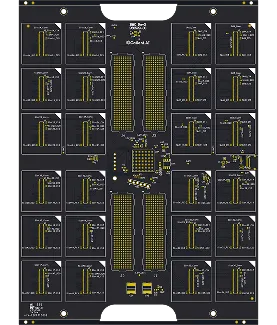
ENIG FR4 PCB Production Record #FR4-20260430-032
| Parameter | Value | Parameter | Value |
|---|---|---|---|
| PCB Type | FR4 PCB | Quantity | 20 pcs |
| Layers | 12 Layers | Board Type | Panel PCB |
| Dimensions | 165.1 x 215.58 mm | Copper Weight | 1oz |
| Thickness | 1.6 mm | Min Track / Spacing | 4/4mil |
| Surface Finish | ENIG (Immersion Gold) | Min Hole Size | 0.3mm↑ |
| Solder Mask | Matte Black | Silkscreen | White |
| Stack-up | Custom | Impedance Control | No |
This 12-layer FR-4 TG170 PCB was produced in a 1×1 panel format with 4 mm process edges on top and bottom. Finished board size is 165.1 × 215.58 mm at 1.6 mm thickness using Shengyi FR-4 material, 1 oz copper on outer layers, 0.3 mm minimum hole size, and 4 mil line width/spacing. The order consisted of 20 pieces with ENIG surface finish, matte black solder mask on both sides, and white silkscreen. No impedance control was required. Production followed standard 100% flying probe testing and mechanical routing.
During DFM review, several engineering questions were resolved to ensure manufacturability. Stackup was adjusted based on our standard 12-layer process capabilities while maintaining the target 1.6 mm thickness. Solder mask clearance issues were addressed where 3 mil openings on traces could not be reliably achieved; these were removed after confirmation. Panelization with optical fiducials and locating holes was verified, and factory markings including UL code and date code were added to the top layer silkscreen as requested. stackup optimization and solder mask clearance handling followed established internal guidelines for this layer count and material.
All files were confirmed prior to release into production. The order completed within the 15-day delivery window with full electrical testing and quality documentation provided. Final boards met dimensional, plating, and cosmetic requirements without deviation, supporting reliable downstream assembly.
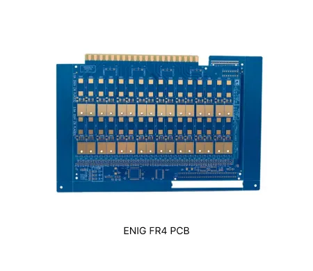
FR4 material with ENIG finish provides balanced electrical performance, shelf life, and assembly compatibility for industrial and high-reliability electronics.
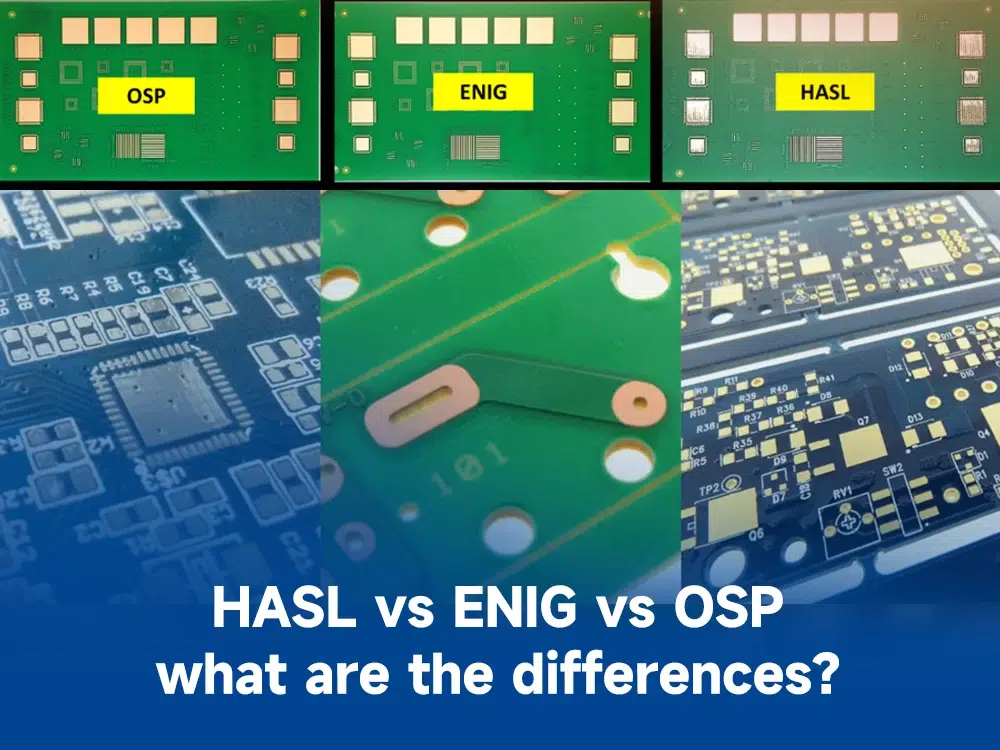
Explore common engineering queries in ENIG, HASL, and OSP FR4 PCBs. Learn real DFM challenges, surface finish compatibility issues, and practical solutions to reduce manufacturing risks and improve yield.
| Order ID | PCB Type | Layers | Dimensions | Solder Mask | Surface Finish | Quantity | Action |
|---|---|---|---|---|---|---|---|
| FR4-20260520-046 | FR4 PCB | 2 | 94.21 x 275 | Green | ENIG (Immersion Gold) | 75 | View detail |
| FR4-20260519-001 | FR4 PCB | 10 | 67.6 x 42 | Green | Gold Plating | 20 | View detail |
| FR4-20260515-068 | FR4 PCB | 14 | 244 x 267 | Green | ENIG (Immersion Gold) | 10 | View detail |


