Introduction
This engineering case examines a 2-layer flexible PCB (FPC) order(#FPC-20260321-066) with 0.2mm finished thickness, OSP surface finish, and demanding panelization requirements. Thin flexible circuits present unique manufacturing challenges compared to rigid boards, particularly in material handling, dimensional stability, and post-processing compatibility.
During CAM review, our team identified significant issues with the customer's requested 1x30 panel array, silkscreen legibility on fine text, and copper thickness confirmation. These concerns are typical for large-format FPC production where material width limitations and shrinkage behavior directly impact yield and downstream SMT assembly.
This real-world case highlights why early EQs are essential in flexible PCB fabrication and how DFM adjustments prevent costly production problems.
Order Overview
The project is a 2-layer flexible PCB using pressed copper construction, measuring approximately 609.6mm x 250mm per unit, with 1oz copper on both sides and 0.2mm overall thickness. Surface finish is OSP, solder mask is white on both top and bottom, and silkscreen is black. Minimum hole size is 0.3mm, with 100% flying probe testing required.
The customer specified a 1x30 V-CUT panelization for 150 pieces (5 sets). However, the combination of wide panel format, thin 0.2mm material, and narrow individual board width (around 8mm effective) created multiple manufacturability conflicts that required immediate engineering clarification.
Main Engineering Questions Found During CAM Review
Large Panelization Feasibility for Thin FPC
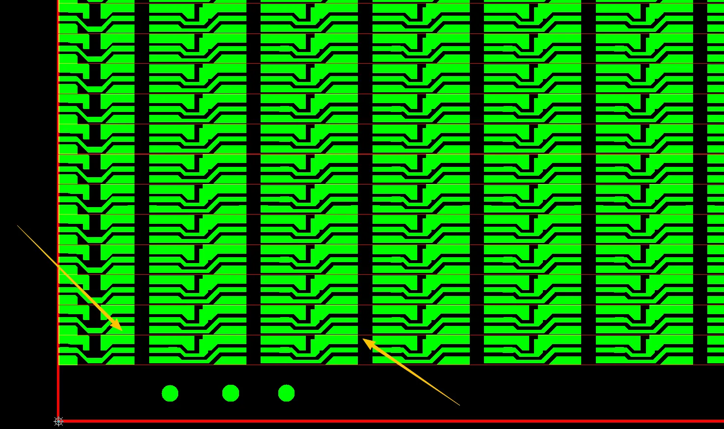
The customer requested a 1x30 panel configuration, resulting in an extremely long and wide array. We noticed that with the flexible material width limitation (effective ~240mm from 250mm roll), this layout left no practical space for tooling/fiducial holes needed for SMT fixtures. Additionally, such a large panel size on 0.2mm FPC makes dimensional stability difficult to control due to material shrinkage during processing.
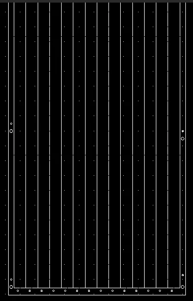
Figure 1: 1x30 panel configuration
Our engineer recommended switching to a more manageable 14pcs per panel (120mm x 619.6mm array). If the original 1x30 layout had been used without adjustment, excessive shrinkage variation could cause misalignment in SMT placement, fiducial recognition failures, and significant yield loss. In extreme cases, the panels could become unprocessable on standard assembly lines, leading to scrap boards and project delays.
We also highlighted that mass production tooling (mold) would not be feasible for the oversized panel, forcing reliance on laser forming which has its own limitations for high-volume runs.
Silkscreen Font Size and Legibility
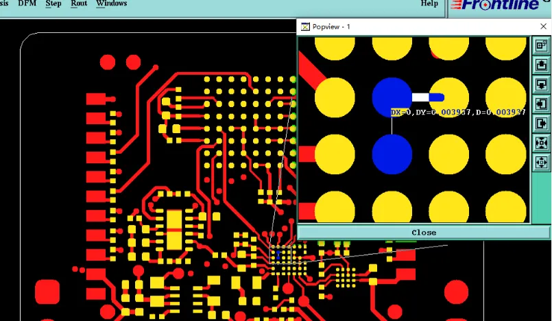
Multiple fine text elements, including small characters under the LOGO, were flagged as too small for reliable reproduction. Our CAM team identified that these features could not be enlarged without affecting layout, leading to a request for customer acceptance of potential character blurring.
![]()
Figure 2: Character blurring
Figure 3: Small characters under the LOGO
We confirmed with the customer using provided reference images showing the expected fuzzy appearance. Proceeding without this confirmation risked customer rejection during incoming inspection for cosmetic reasons or readability issues in final product marking. According to typical IPC-A-600 criteria for marking legibility, such fine features on flexible substrates require careful evaluation.
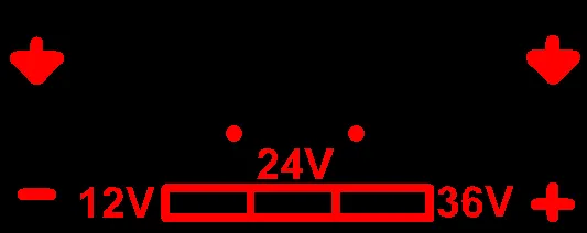
Copper Thickness and Stackup Confirmation
Although the order specified 1oz copper, the customer requested confirmation for 1.5oz finished copper thickness. Our engineer reviewed the stackup to ensure compatibility with the ultra-thin 0.2mm construction. Mismatched copper weight expectations could affect etching uniformity and final thickness control on flexible material.
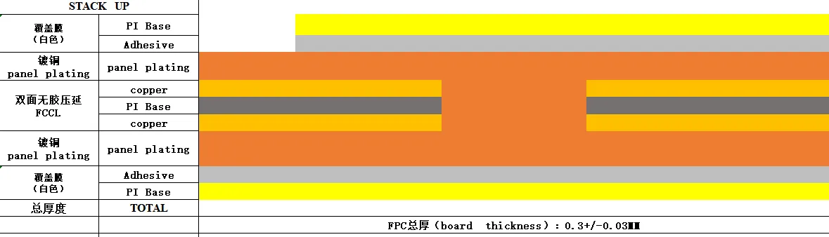
Figure 4: Copper Thickness and Stackup info
Ignoring this would risk boards delivered with incorrect copper thickness, impacting current carrying capability, flexibility, and potentially causing open or short circuits due to over-etching.
Suggested EQ Categories
Panelization & Process Optimization
- 1x30 array feasibility on thin FPC material
- Tooling hole space and SMT compatibility
- Alternative 14pcs panel proposal
Solder Mask & Silkscreen Issues
- Fine text legibility and blurring acceptance
File & Manufacturing Data Issues
- Copper thickness/stackup confirmation
- Multiple production file verifications
Manufacturing Risks and DFM Insights
Flexible PCBs are particularly sensitive to panel size. Oversized arrays on thin material amplify shrinkage effects, making registration and handling challenging. Without early intervention, this often results in distorted panels that fail SMT fiducial alignment or require manual processing, driving up costs and reducing yield.
Silkscreen issues on FPC frequently stem from designers not accounting for the limitations of flexible substrates and white solder mask combinations. Blurred or incomplete marking can lead to traceability problems in the field or outright rejection.
If these EQs were ignored, consequences could include complete production stoppage due to unmanufacturable panels, excessive scrap from dimensional instability, assembly line downtime, and repeated revision cycles.
How the Engineering Team Resolved the Issues
Our CAM engineer prepared alternative panelization drawings using the 14pcs configuration with proper tooling holes. We provided clear reference images for the expected silkscreen appearance and confirmed the copper thickness requirements against the stackup.
After multiple file confirmation rounds and customer approval of the blurred text samples, we finalized the production data. "We always push for practical panelization on thin FPCs," our senior CAM engineer noted, "because forcing oversized arrays almost always leads to handling and registration failures later."
Final Manufacturing Outcome
All engineering clarifications were completed successfully. The customer accepted the revised 14pcs panel proposal, confirmed acceptance of the silkscreen character appearance, and verified copper thickness parameters. Updated production files were approved, and the order was released for fabrication.
Key Takeaways for PCB Designers
- For flexible PCBs, consult with your fabricator early on panelization — large arrays often exceed practical material and process limits.
- Account for effective material width and required tooling space when designing multi-up panels for FPC.
- Design silkscreen text with sufficient minimum size, especially on white solder mask flexible boards, to ensure legibility.
- Clearly specify and confirm copper weight targets, as finished thickness on thin FPC is highly process-dependent.
- Provide reference images when accepting cosmetic variations like character blurring.
- Prepare for multiple file confirmation rounds on complex FPC jobs to align expectations.
- Balance panel quantity per sheet against shrinkage control and SMT compatibility.
FAQ
Q1: Why is large panelization problematic for thin flexible PCBs?
A1: Thin FPC material (0.2mm) has high shrinkage variation. Oversized panels become difficult to handle, register accurately, and process through SMT lines, often resulting in misalignment or physical damage.
Q2: Can small silkscreen text be reliably produced on FPC?
A2: Very fine text often results in blurring or incomplete formation due to material flexibility and ink behavior. Fabricators may request acceptance of minor fuzziness to avoid layout changes.
Q3: What space is needed for SMT tooling on FPC panels?
A3: Adequate margin around the array is required for fiducials and fixture holes. Narrow boards packed densely (e.g., 30-up) frequently leave insufficient room, complicating automated assembly.
Q4: Why confirm copper thickness separately on FPC?
A4: Flexible materials react differently during plating and etching. Final copper weight must align with both electrical and mechanical (bend radius) requirements.
Q5: How does early DFM review benefit FPC projects?
A5: It prevents unmanufacturable panel designs, reduces scrap from dimensional issues, and ensures compatibility with assembly processes before production begins.