In PCB manufacturing, even seemingly straightforward 6-layer boards can present multiple manufacturability challenges during CAM engineering review. This case study examines a real production order (#FR4-20260420-071) involving a compact 56 × 31 mm FR-4 board with TG150 material, 1.6 mm finished thickness, and impedance requirements. Our CAM team identified several critical DFM issues that required customer clarification before releasing the job to production.
This article details the engineering questions raised, the underlying manufacturing reasons, potential risks if left unaddressed, and how our team resolved them. Such reviews are standard practice to prevent scrap, ensure yield, and align design intent with actual fabrication capabilities.
Order Overview
The project is a 6-layer FR-4 board using KB-6165F material with TG150 rating. Finished board thickness is 1.6 mm, with 1 oz copper on both outer and inner layers. Minimum hole size is 0.2 mm, and the design includes controlled impedance requiring a full test report. Surface finish is lead-free HASL, with green solder mask on both sides and white silkscreen. Panelization is 1×2 using stamp holes, with a total order quantity of 10 pieces (5 sets). Delivery time was set at 18 days.
The Gerber data included impedance specifications, and the board featured standard 100% flying probe testing. While the stackup was relatively conventional, the combination of tight tolerances, panelization details, and edge proximity of features triggered multiple engineering clarifications during our standard DFM review process.
Main Engineering Questions Found During CAM Review
1. Panelization Inconsistency and Stamp Hole Confirmation
One of the first issues our CAM engineer identified was a mismatch between the customer's provided panel drawing and our standard fabrication panelization. The customer data showed different overall panel dimensions compared to our optimized 1×2 layout using stamp hole connections.
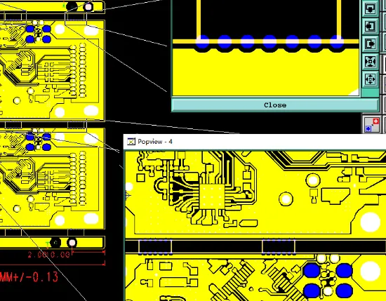
Figure 1: Standard panel drawing with stamp holes
We noticed that using the customer's original panel size could lead to inefficient material utilization and potential handling issues during processing. Our engineer suggested adopting our standard panel drawing with stamp holes for better mechanical stability during routing and depanelization. We asked the customer to confirm if our proposed panel layout was acceptable.
If ignored, mismatched panelization could result in irregular board edges, increased risk of chipping during separation, or even misalignment in downstream SMT processes. In extreme cases, this leads to scrap boards or assembly line stoppages due to dimension variations.
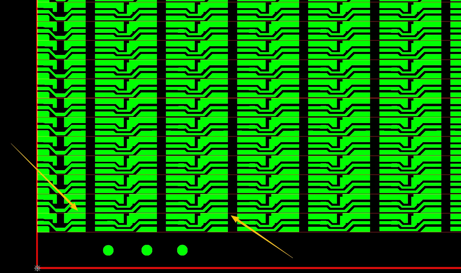
2. Trace Width Compensation and Hole-to-Line Clearance
A significant DFM concern involved minimum hole-to-line spacing. The original design specified 0.15 mm in some areas. After applying standard manufacturing compensation for etching and plating, the effective clearance dropped below safe limits. Our CAM team proposed reducing specific trace widths from 0.15 mm / 0.2 mm down to 0.1 mm to restore adequate clearance.
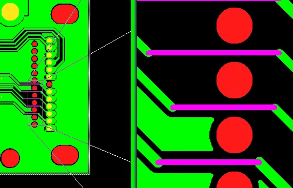
Figure 2: Reduce specific trace widths from 0.15 mm / 0.2 mm down to 0.1 mm
We noticed during data preparation that without this adjustment, the risk of copper shorts or incomplete etching would be high, particularly around the 0.2 mm holes. According to typical IPC-2221 spacing guidelines for this class of board, the compensated values were approaching manufacturability limits.
If the EQ had been ignored and production continued without adjustment, we could have seen short circuits between traces and hole walls, etching residuals, or open circuits after plating. This would directly translate to low yield and potential field failures due to unreliable interconnections.
3. Inner Layer Copper Thickness Confirmation
There was inconsistency in customer feedback regarding inner layer copper weight. Initial communications suggested possible deviation from the standard 1 oz across all layers. Our engineer requested explicit confirmation that inner layers should follow the outer layer specification of 1 oz Cu.
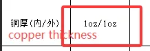
Figure 3: Standard 1 oz across all layers
This clarification is critical because copper thickness directly affects impedance control, etching parameters, and overall board thickness tolerance. We noticed during stackup review that any mismatch could invalidate the provided impedance structure.
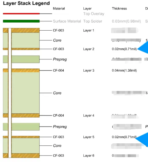
Figure 4: Layer stack legend
Proceeding without confirmation risks incorrect impedance values, leading to signal integrity problems in the final application, or even delamination if plating and pressing parameters are based on wrong assumptions.
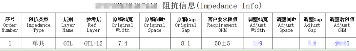
Figure 5: Impedance info
4. Holes Near Board Edge and Potential Breakout / Exposed Copper
Several holes were positioned very close to the board edge. After accounting for routing and V-score tolerances (where applicable), our analysis showed a high likelihood of minor breakout, potentially exposing copper on the finished edge.
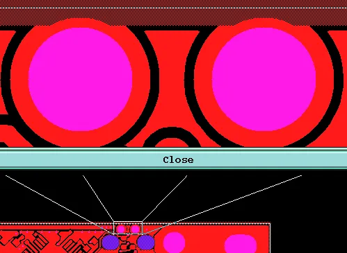
Figure 6: Holes near board edge
Our CAM engineer flagged this and asked the customer to confirm acceptance of slight exposed copper or ring breakout in these locations. We explained that while the hole wall would retain copper, edge proximity made full annular ring preservation challenging per standard routing tolerances.
If not clarified, this could result in cosmetic defects, edge shorting risks during assembly, or corrosion over time in harsh environments. Based on IPC-A-600 acceptability criteria, exposed copper near edges increases defect classification risk.
5. Silkscreen Character Size and Solder Mask Openings
The design featured relatively small silkscreen characters in some areas. Our review indicated that after processing, these might appear incomplete or fuzzy on the finished board.
Figure 7: Small silkscreen characters in some areas
Additionally, there were extra openings on the SMD layer compared to solder mask layers that required confirmation to follow original data.
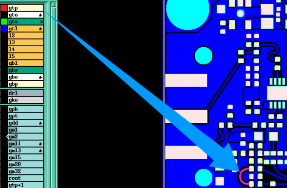
Figure 8: Extra openings on the SMD layer
We asked the customer to confirm acceptability of potential legibility issues and the extra SMD openings. Minor issues like these are common but can affect assembly if component markings become unclear.
Suggested EQ Categories
File & Manufacturing Data Issues
- Panelization dimension mismatch between customer and factory files
- Silkscreen legibility concerns
Hole & Tolerance Issues
- Hole-to-line clearance after compensation
- Holes near board edge and breakout risk
Stackup & Material Issues
- Inner layer copper thickness confirmation
- Impedance structure verification
Panelization & Process Optimization
- Stamp hole panel confirmation
Manufacturing Risks and DFM Insights
This case highlights several recurring DFM pitfalls in compact multilayer designs. Tight hole-to-trace clearances are particularly problematic because etching compensation and plating tolerances consume design margins quickly. Without adjustment, yield drops significantly due to shorts or opens.
Edge proximity issues are another common trigger. Our experience shows that holes placed too close to the final board outline often lead to breakout, especially on smaller panels. Ignoring this can cause immediate cosmetic failures or long-term reliability problems such as copper peeling at edges.
Panelization mismatches waste time in multiple review cycles and risk mechanical damage during depanelization. In this order, confirming stamp hole usage prevented potential handling defects.
Overall, these issues demonstrate why factories raise EQs: to protect both parties from scrap and delays. Unresolved, they could lead to board warpage from improper copper balance, via cracking under thermal stress, or signal instability from off-spec impedance.
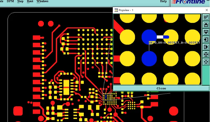
How the Engineering Team Resolved the Issues
Our engineering team worked closely with the customer to address each point. For the trace compensation, we provided marked-up images showing proposed adjustments and received approval to proceed with the reduced widths. This maintained electrical performance while ensuring manufacturability.
After reviewing the stackup, we confirmed inner layers at 1 oz and verified the impedance structure against the provided confirmation document. The panel drawing was updated to our standard with stamp holes, which the customer approved.
For edge holes, the customer accepted the possibility of minor exposed copper, allowing us to optimize routing parameters accordingly. Silkscreen concerns were noted, with a recommendation for future designs to increase character size where possible.
Throughout the process, our CAM engineer maintained clear communication with annotated screenshots, reducing ambiguity and speeding up the clarification cycle.
Final Manufacturing Outcome
All engineering questions were resolved through customer confirmation. The data was updated with approved adjustments to clearances, panelization, and stackup parameters. CAM files were finalized, and the order was released for production with impedance testing and full quality documentation as specified. This proactive review helped ensure the 10-piece run met both design and manufacturing requirements.
Key Takeaways for PCB Designers
- Provide clear panelization drawings early and align dimensions with factory capabilities to avoid multiple revisions.
- Maintain adequate hole-to-trace clearances (typically >0.2 mm post-compensation) and specify minimum trace widths considering etching factors.
- Position holes with sufficient margin from board edges (at least 0.3-0.5 mm depending on process) to prevent breakout and exposed copper.
- Confirm copper weights for all layers explicitly, especially in impedance-controlled designs.
- Use standard layer naming and include detailed fabrication notes to reduce misinterpretation during CAM review.
- Design silkscreen characters with sufficient size and consider solder mask defined vs. copper defined pads consistently.
- Submit impedance requirements with clear stackup diagrams and reference structures for accurate modeling.
- Review Gerber data for consistency between solder mask and paste layers before submission.
FAQ
Q1: Why do PCB factories adjust trace widths during CAM review for hole-to-line clearance?
A1: Etching and plating processes require compensation that reduces effective spacing. Without adjustment, shorts or etching defects occur. Our team reduces trace width where necessary to restore safe clearance while preserving functionality.
Q2: What risks arise from holes placed too close to the board edge?
A2: Minor breakout can expose copper or damage annular rings, leading to edge shorts, corrosion, or mechanical weakness. Accepting limited exposure or increasing margin prevents these issues.
Q3: Why is inner layer copper thickness confirmation important for multilayer boards?
A3: It affects impedance calculations, board thickness, and etching parameters. Mismatches can invalidate controlled impedance and cause signal integrity problems or delamination.
Q4: How does panelization affect PCB manufacturing quality?
A4: Incorrect panel size or connection methods (like stamp holes) can cause handling damage, uneven stress during routing, or poor material utilization. Standardized panelization improves yield and consistency.
Q5: Can small silkscreen characters be reliably produced on dense boards?
A5: Very small characters risk becoming incomplete or blurred after processing. Designers should aim for minimum heights recommended by IPC standards or confirm with the manufacturer for critical markings.
Q6: What is the purpose of impedance structure confirmation in multilayer PCBs?
A6: It ensures the fabricated stackup matches simulation models. Our team verifies dielectric thicknesses, copper weights, and layer order before production to guarantee electrical performance.