6 Layer FR4 PCB Production Record #FR4-20260420-071
| Parameter | Value | Parameter | Value |
|---|---|---|---|
| PCB Type | FR4 PCB | Quantity | 10 pcs |
| Layers | 6 Layers | Board Type | Panel PCB |
| Dimensions | 56 x 31 mm | Copper Weight | 1oz |
| Thickness | 1.6 mm | Min Track / Spacing | 6/6mil↑ |
| Surface Finish | HASL Lead Free | Min Hole Size | 0.2mm |
| Solder Mask | Green | Silkscreen | White |
| Stack-up | Default | Impedance Control | Yes |
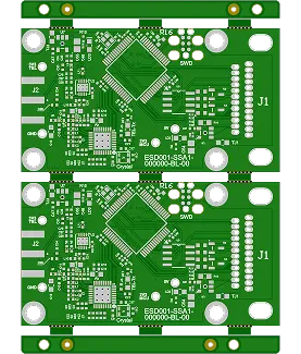
This 6-layer FR-4 PCB order consisted of 10 pieces (5 sets) with a finished board size of 56 × 31 mm and 1.6 mm thickness using standard 1 oz copper on both inner and outer layers. Production utilized lead-free HASL surface finish, green solder mask, and white silkscreen, with a minimum hole size of 0.2 mm and 6 mil trace width/spacing. Impedance control was required per the provided stack-up, and the panels were arranged 1×2 with stamp hole connections. The order followed a standard 18-day delivery timeline with 100% flying probe testing.
During DFM review, several issues required clarification and adjustment. The customer's paste layer openings exceeded the solder mask, which was confirmed for production as per original design. Panelization dimensions differed between files; the final layout adopted stamp hole connections as specified. Trace compensation was applied where original 0.15 mm hole-to-line clearance became insufficient after process allowances, with trace widths locally adjusted to 0.1 mm after confirmation. Small silkscreen characters were noted as potentially incomplete on the finished board. Holes near the board edge were highlighted for minor breakout risk with possible copper exposure, which the customer accepted along with standard annular ring requirements.
All engineering adjustments, including panelization and trace compensation, were implemented prior to inner layer imaging to maintain impedance integrity and mechanical reliability. The boards were successfully completed with consistent electrical performance and delivered on schedule, demonstrating stable execution of multi-layer FR-4 processing with impedance requirements.
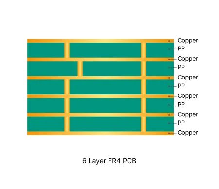
Six layer FR4 boards provide optimized routing density and power distribution. They require precise lamination and plating process control to maintain yield and reliability.

In-depth guide to the most frequent Engineering Queries (EQ) and DFM issues in Multilayer FR4 PCB (4/6/8+ layers) production. Real factory insights on stack-up confirmation, impedance control, copper balance, inner layer design, via treatment, registration, and practical prevention strategies.
| Order ID | PCB Type | Layers | Dimensions | Solder Mask | Surface Finish | Quantity | Action |
|---|---|---|---|---|---|---|---|
| FR4-20260528-028 | FR4 PCB | 2 | 185 x 245 | Green | HASL Lead Free | 5 | View detail |
| FR4-20260526-001 | FR4 PCB | 2 | 100 x 100 | Green | HASL Lead Free | 10 | View detail |
| FR4-20260525-001 | FR4 PCB | 2 | 50 x 45 | Matte Green | HASL Lead Free | 20 | View detail |


