The order or panel note calls for panelization. The board files released with that note — outline, drill, outer copper, and solder mask — never place a tooling hole or a fiducial mark on the individual board. The package therefore asks for a panel without saying where fabrication should register the array, or where assembly should look for a vision target.
That mismatch is what generates the EQ. We draw tooling holes and fiducial marks on the process edge and send the sketch back: panel production is required; please confirm the panel. When the PCS drill list has no positioning hole, the same sketch is more specific — four tooling holes specified as 2.0 mm and four fiducial marks specified as 1.0 mm on the rail. Sometimes the locations are acceptable and the mark itself is not. The solder mask opening over the fiducial is large enough that copper around the mark sits open.
The CAM question is which file defined the holes and marks, what the overlay at each site can prove, and whether the factory panel sketch may stay.
| Released condition | What the package actually shows | What has to be confirmed |
|---|---|---|
| Panelization required; PCS has no tooling holes or fiducial marks | The order or panel note asks for a panel. Outline, drill, copper, and solder mask do not place either feature on the board. | Whether factory-added tooling holes and fiducial marks on the process edge may stay, and where. |
| No positioning holes inside the PCS | The factory sketch adds four tooling holes specified as 2.0 mm and four fiducial marks specified as 1.0 mm on the process edge. | Whether that set is accepted, relocated, or replaced by features on the PCS. |
| Fiducial solder mask opening is large | The copper of the mark is present. The solder mask opening around it leaves nearby copper exposed. | Whether the opening is intended vision clearance, should be pulled back to the mark, or the mark should move. |
A tooling hole is a drilled registration hole. A fiducial mark is copper with a solder mask opening so assembly vision can see it. They are not interchangeable, and neither one is a stamp hole, a PTH, or a silk symbol.
PCB Panelization: When the PCS Has No Tooling Holes or Fiducial Marks
Start with the order and any panel drawing. If the text only says the boards will be arrayed as part of PCB panelization, it has not named a tooling-hole tool, a hole site, a fiducial copper flash, or a solder mask opening over that flash.
Then read the board. The outline is the finished PCS. The drill list is every hit the designer released. Outer copper and solder mask show every land and every opening. When none of those files place a tooling hole or a fiducial mark on the PCS, and the customer did not release a rail that already carries them, the panel note and the Gerber set disagree about registration.
A drill hit already on the board does not become a tooling hole just because the job is now a panel. Component holes, vias, and stamp-hole rows stay what the tool list says they are. A round copper pad does not become a fiducial mark just because it is circular. The mark still needs the copper, a solder mask opening over it, and a drawing or note if the designer meant a vision target rather than a land.
Putting PCB tooling holes and fiducial marks on the process edge because the job is a panel is a factory proposal, not an approved panel definition. That is the EQ we send when the note asks for panel production and we attach a sketch with positioning holes, optical points, and rail copper: confirm whether this is the panel the customer wanted.
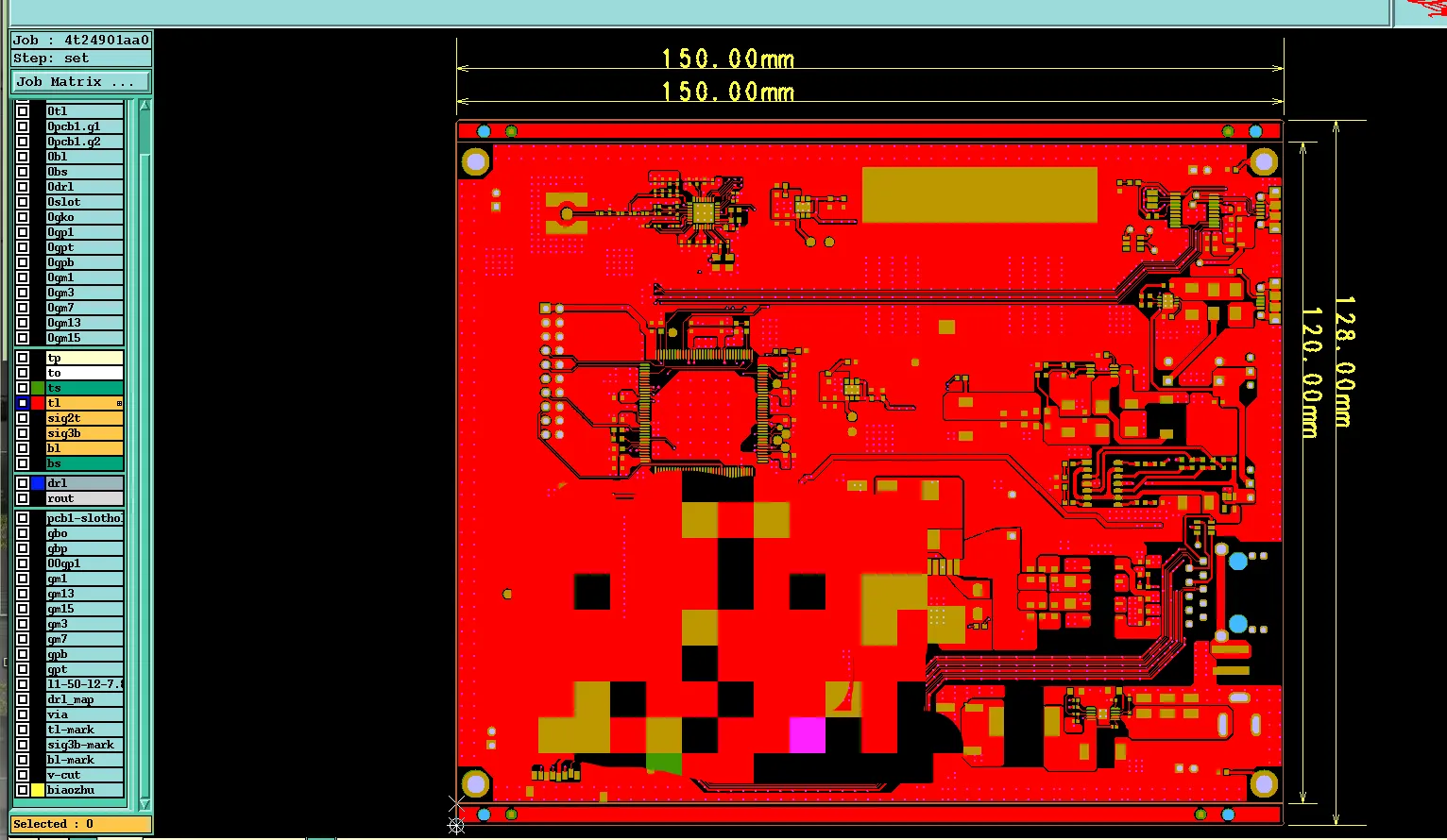
As shown, tooling holes, fiducial marks, and copper thieving have been added to the Edge Rail per standard practic
Drill, Copper, and Solder Mask at Each Tooling Hole and Fiducial Mark
The overlay is checked at each tooling-hole and fiducial-mark site, not only at the panel level.
At a proposed tooling hole, the drill layer shows whether a hit exists and which tool it uses. The outline shows whether that hit sits on the process edge, inside the PCS, or on the board contour. Copper and solder mask at a tooling hole matter only when they collide with the hole. The hole itself is the registration object.
At a proposed fiducial mark, outer copper shows the flash. Solder mask shows whether that flash is open. The factory sketch shows where we placed the mark relative to the outline and the array. Paste is not required at the mark. Silk next to the mark is not the mark.
| Object | Overlay can show | Overlay cannot show |
|---|---|---|
| Tooling hole | The drill hit, the tool, and whether the site is on the process edge, on the PCS, or on the outline. | Whether the customer intended that hole, or only intended panelization. Whether the 2.0 mm diameter on the sketch is the size the assembler will pin. |
| Fiducial mark | The copper flash, the solder mask opening over that copper, and the sketch location relative to the array. | Whether assembly needs panel fiducials, local fiducials on each PCS, or both. Whether the 1.0 mm mark on the sketch is the size the assembler will use. Whether a large opening is intended clearance or copper that should stay covered. |
| Factory panel sketch | Where we drew the holes and marks, and whether rail copper is bundled next to them. | That the sketch is the released panel drawing. Rail pour itself belongs with the process-edge review, not with the fiducial. |
A feature on the factory sketch is not the same as a feature the customer released. Missing holes and marks are one question. Solder mask versus copper at the fiducial is another. Accepting the sketch locations does not close the opening.
No Tooling Holes Inside the PCS — Fiducial Marks Only on the Process Edge
"No tooling hole inside the PCS" is a drill-to-outline fact. It is not a verdict that the board is wrong.
The factory proposal in that EQ is specific: four PCB tooling holes and fiducial marks specified as 2.0 mm and 1.0 mm respectively, all on the process edge, because the PCS has no positioning hole. Those numbers stay inside the EQ. They are not published here as standard PCB tooling hole design or standard fiducial design.
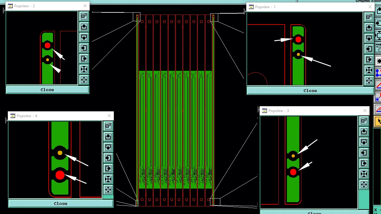
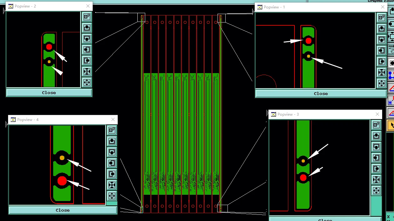
As shown in the image, since there are no positioning holes on the PCB, we have added four 2.0 mm tooling holes and four 1.0 mm fiducial marks on the panel rails.
Count and side matter as much as size. Four tooling holes and four fiducial marks on the rail is one construction. Local fiducial marks on each PCS is another. Panel fiducials and local fiducials are not the same object, and the files do not say which set assembly will run.
A 1.0 mm "mark point" is still a fiducial mark: copper plus a solder mask opening. A silk cross, or a copper pad still covered by mask, is not a vision target.
Confirm that the PCS drill list has no tooling-hole tool on the board. Show the four hole sites and the four fiducial-mark sites on the process edge. Ask the customer to accept that set, move it, or place tooling holes and fiducial marks inside the PCS.
Fiducial Marks Whose Solder Mask Opening Exposes Nearby Copper
A fiducial mark that assembly can see is copper with a solder mask opening over it. Once the locations are accepted, the fiducial solder mask opening at the mark can still be wrong.
Overlay of fiducial-mark copper against solder mask at that site shows two mismatches that look similar on the screen and are not the same instruction.
The opening may simply be larger than the fiducial copper, so extra copper or laminate around the mark is visible. That can be the clearance the assembler wanted, or leftover expansion from a copied land rule.
The opening may also reach adjacent traces or plane copper that the designer never drew as part of the mark. That is exposed copper around the fiducial, not extra clearance on the mark itself.
The overlay shows the mismatch. It does not show which of those two the artwork meant. Keeping the process-edge locations does not keep the opening. Compare the fiducial copper with the solder mask opening, and check whether the opening also uncovers nearby pour or traces. Ask whether to keep the opening, pull it back to the fiducial copper, or move the mark off the adjacent copper.
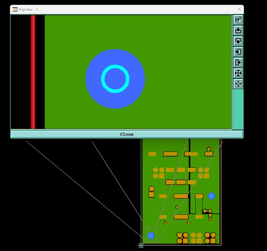
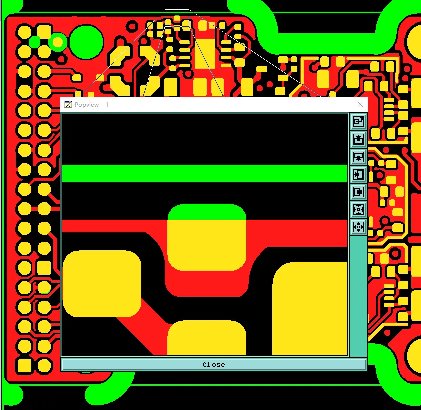
The fiducial hole solder mask opening is larger, which cause the nearby copper exposed.
Keep the Tooling Holes and Fiducial Marks, Relocate Them, or Change the Opening
The panel is not rewritten on a silent assumption. Location and solder mask opening can both stay open on the same job.
| Finding | If confirmed | If rejected |
|---|---|---|
| Tooling holes and fiducial marks added on the process edge for panelization | Keep the factory panel sketch as the working panel definition. | The customer supplies locations, or points to features already on the PCS that CAM missed. |
| No tooling holes inside the PCS; four 2.0 mm holes and four 1.0 mm fiducial marks on the rail | Accept that set as drawn. | Relocate, change the count, place features on the PCS, or drop the added rail features. |
| Fiducial-mark solder mask opening exposes copper | Keep the opening as released. | Pull the opening back to the fiducial copper, or move the mark off adjacent copper. |
The factory sketch does not become Gerber until someone accepts it. The added tooling holes and fiducial marks are not deleted until someone rejects them. Write the EQ against the sketch plus three file objects: the tooling-hole drill hit, the fiducial-mark copper, and the solder mask opening. Record the close on the panel drawing or in the order note.
Panel Drawing Still Silent on Tooling Holes and Fiducial Marks
The same gap can be caught before the EQ goes out.
The order asks for panelization and never names tooling holes or fiducial marks. The features may belong on the process edge, inside the PCS, or both — the panel drawing has to say which. Each tooling hole needs a drill tool and a site off the finished-board outline unless the customer is placing a tooling hole on the PCS on purpose. Each fiducial mark needs copper and a solder mask opening, not only a silk symbol. The solder mask opening has to be checked for exposed copper around the mark before the sketch is treated as closed.
If CAM adds tooling holes or fiducial marks, that addition stays an EQ with a sketch. Run the same overlays on the package the customer believes they already released.
FAQ
Q1: What are fiducial marks on a PCB?
A1: A fiducial mark is a copper feature with a solder mask opening over it so assembly vision can locate the panel or the individual board. Paste is not required at the mark. A silk symbol without open copper is not a fiducial mark. Panel fiducials on the process edge and local fiducials on each PCS are different placements of the same kind of object.
Q2: What are tooling holes in PCB panelization?
A2: A tooling hole is a drilled registration hole used to pin the panel during fabrication or assembly handling. It is not a fiducial mark, not a stamp hole, and not a component hole. When the PCS drill list has no such hole and the job is a panel, CAM often proposes tooling holes on the process edge and asks the customer to confirm the sketch.
Q3: What is the difference between a tooling hole and a fiducial mark?
A3: The tooling hole is a drill hit. The fiducial mark is copper plus a solder mask opening. One is for pin registration. The other is for vision. A package that only asks for panelization has defined neither until a drawing, a note, or a confirmed factory sketch places them.
Q4: Where should fiducial marks and tooling holes go on a panel?
A4: On the process edge, on the PCS, or both — whichever the panel drawing and the assembler require. "Panelize" is not a location list. If the factory adds four tooling holes and four fiducial marks on the rail because the PCS has none, that set is a proposal until it is accepted or replaced.
Q5: What is the recommended size for a PCB fiducial mark?
A5: This review does not publish a recommended size. The 1.0 mm fiducial marks in the EQ are the values specified on that factory sketch, not a design rule. They close only if the customer accepts them. A customer panel drawing or an assembler requirement can call a different copper size and a different solder mask opening.
Q6: Why does the solder mask opening around a fiducial mark leave exposed copper?
A6: The opening is larger than the fiducial copper, or it reaches nearby pour or traces. Overlay shows the mismatch. It does not show whether that extra open copper is intended vision clearance. Confirm keep, pull the opening back to the mark, or move the mark.
Q7: Where should fiducials be placed on a PCB design?
A7: On the process edge, on the PCS, or both — whichever the panel drawing and the assembler require. Local fiducials belong with the land pattern they serve. Panel fiducials belong with the array. The released files have to show the copper and the solder mask opening at those sites. “Panelize” is not a placement list, and a factory sketch that puts marks on the rail is a proposal until it is accepted or replaced.