In this real-world engineering review from our CAM department, we processed a 4-layer 1.0mm FR-4 TG170 board with ENIG finish and 2oz copper. What started as a standard order quickly revealed several critical DFM issues that required immediate clarification with the customer. This case demonstrates why thorough CAM engineering review remains essential even for seemingly straightforward multilayer PCBs.
Introduction
During the CAM review of the order (#FR4-20260402-041), our engineering team identified multiple manufacturability concerns involving stackup definition, panelization dimensions, solder mask openings, and silkscreen placement. These issues are common in 4-layer designs where designers often rely on default fabrication notes or overlook factory-specific process constraints.
We noticed early in the review that the customer-provided stackup conflicted with our standard high-TG process capabilities. Additionally, the panelization layout with 4mm process edges produced a final panel dimension different from the fabrication note. Silkscreen elements overlapping solder mask openings and oversized optical point windows further complicated the review. Our CAM engineer flagged these items to prevent production risks such as board thickness deviation, exposed copper, and potential assembly problems.
This case study walks through the actual engineering questions (EQs) raised, the manufacturing reasoning behind them, and the resolution steps taken. It highlights the gap between design intent and real production constraints in modern PCB fabrication.
Order Overview
This was a 4-layer FR-4 PCB using TG170 material, finished board thickness of 1.0mm, with 2oz copper on both outer layers. The board size measured 33.91mm × 84.52mm. Surface finish was ENIG (Immersion Gold), with black solder mask on both sides and white silkscreen. Minimum hole size was specified at 0.3mm, and the order required 100% flying probe testing.
Panelization was set to 2×1 with 4mm process edges on top and bottom. The customer requested V-scoring for depanelization. No blind or buried vias were indicated in the primary stackup, though resin plugging was mentioned for certain via sizes in the fabrication notes. Production was planned for mechanical forming with a 15-day lead time.
While the parameters appeared routine for a 4-layer high-TG board, the combination of specific stackup requirements, panelization details, and artwork elements triggered several targeted engineering clarifications during our DFM review.
Main Engineering Questions Found During CAM Review
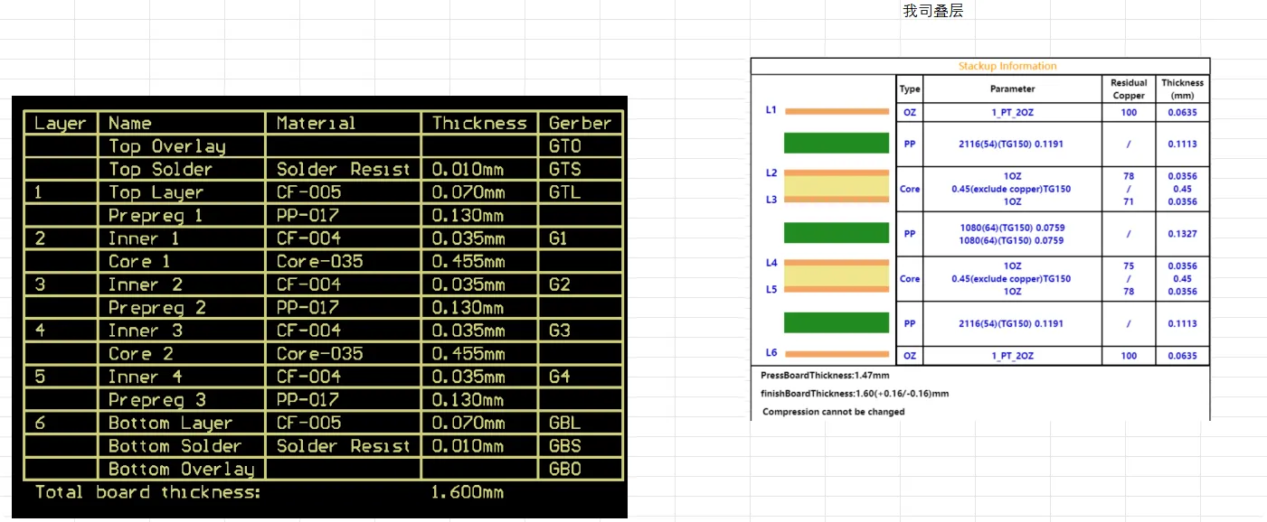
1. Stackup and Finished Board Thickness Conflict
Our engineer identified an inconsistency between the customer's specified stackup structure and the target finished board thickness of 1.0mm. After reviewing the provided layer press chart against our standard TG170 material tolerances, we determined that adjustments were necessary to meet both the electrical and mechanical requirements.
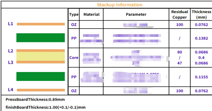
Figure 1: Specified stackup structure

Figure 2: Board thickness requirement
We noticed that following the customer's original stackup exactly would likely result in a finished thickness outside the acceptable tolerance range for a 1.0mm board. To reduce manufacturing risk, our engineering team recommended a minor adjustment to the dielectric thicknesses while maintaining the overall impedance characteristics and 2oz copper weights.
If this had been ignored, the board could have ended up with excessive or insufficient thickness, leading to assembly fit issues, potential warpage during reflow, or failure to meet mechanical specifications in the final product enclosure. According to typical IPC-6012 Class 2 tolerances, such deviation could result in scrap or costly re-engineering at the assembly stage.
2. Panelization Dimension and Process Edge Mismatch
The customer requested 2×1 panelization with 4mm process edges on the top and bottom directions. However, when our CAM team applied this configuration, the resulting panel dimensions measured 67.56mm × 92.46mm, which did not match the size noted in the fabrication instructions.
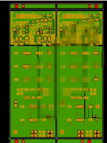
Figure 3: Requested 2×1 panelization diagram
Our engineer suggested confirming the intended final panel size and V-cut positioning. This discrepancy is critical because incorrect panelization can affect routing efficiency, material utilization, and depanelization quality. We confirmed the 4mm process edge requirement but aligned the overall panel to the actual Gerber data to avoid edge copper exposure after V-scoring.
If left unaddressed, this mismatch could have caused exposed copper along the V-cut lines after depanelization, increasing the risk of edge short circuits during assembly or handling. In severe cases, it leads to cosmetic defects or functional failures in high-density edge connector areas.
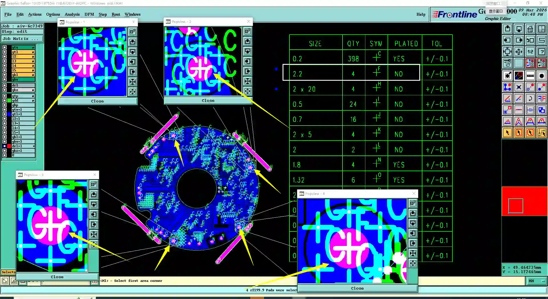
3. Solder Mask Openings and Exposed Copper Risk
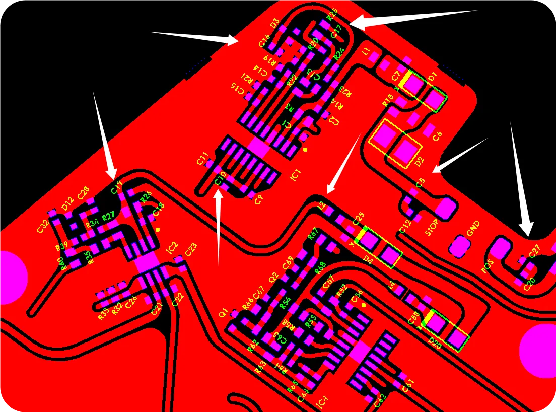
We identified that the optical alignment points (fiducials) had oversized solder mask windows, resulting in exposed copper around the perimeter. Additionally, several silkscreen characters were positioned directly over via pads and solder mask openings.

Figure 4: The oversized solder mask window
Our CAM engineer confirmed that such large openings could lead to unintended copper exposure after ENIG processing. We recommended either reducing the window size or adjusting the mask expansion to maintain proper coverage while preserving alignment functionality. For the silkscreen characters overlapping pads, we proposed complete removal as they would be etched away during mask processing anyway.
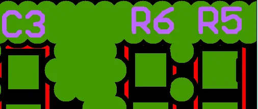
Figure 5: Silkscreen characters overlapping pads
Ignoring this would likely produce boards with exposed copper near fiducials, potentially causing solder bridging during SMT assembly or long-term reliability issues due to oxidation. Based on IPC-A-600 acceptability criteria, excessive exposed copper near process edges or critical areas is a common cause of yield reduction.
4. Resin Plugging Specification vs Actual Gerber Data
The fabrication notes called for resin plugging on 8mil vias, yet our review of the Gerber files found no vias of that exact size. This mismatch required clarification to determine whether the plugging requirement applied to the nearest via sizes or if it was a specification error.
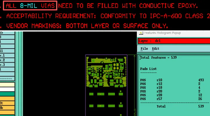
Figure 6: Mismatch between fabrication note for resin plugging on 8mil vias and Gerber files
After confirmation, we aligned the plugging process with existing via dimensions to avoid unnecessary operations that could introduce resin voids or plating defects.
Suggested EQ Categories
Stackup & Material Issues
- Finished thickness vs. customer stackup conflict
- TG170 material press adjustment recommendation
Panelization & Process Optimization
- 2×1 panel dimension mismatch with process edges
- V-cut positioning and 4mm edge confirmation
Solder Mask & Silkscreen Issues
- Oversized fiducial mask windows causing exposed copper
- Silkscreen legend boxes overlapping pads and openings
Hole & Tolerance Issues
- Resin plugging specification vs. actual via sizes in Gerber
Manufacturing Risks and DFM Insights
This case reinforced several recurring DFM challenges we see in 4-layer high-TG designs. Customers frequently provide stackup diagrams that do not account for actual prepreg and core thickness variations available in the factory. Panelization instructions often fail to consider the combined effect of process edges and scoring lines on final dimensions.
Silkscreen elements placed without considering solder mask expansion are another common trigger. If ignored, these issues can lead to multiple production delays, increased engineering communication cycles, and higher scrap risk. In one similar past case, unaddressed panel dimension mismatch resulted in copper peeling along V-cut edges after assembly, causing functional failures in the field.
How the Engineering Team Resolved the Issues
Our team worked closely with the customer through multiple file iterations. For the stackup, we provided a recommended press chart that achieved the 1.0mm target thickness while preserving the intended layer ordering. The customer approved the adjustment after reviewing the impedance implications.
Panelization was standardized to the actual Gerber-derived dimensions with clear 4mm process edges confirmed. Silkscreen legend boxes were fully removed as they overlapped mask openings and would not survive production. Fiducial mask windows were optimized to balance alignment accuracy and copper coverage.
Throughout the process, we maintained detailed version control and provided annotated screenshots for every change. This collaborative approach prevented unnecessary delays and ensured the final production data met both design intent and manufacturing capability.
Final Manufacturing Outcome
After receiving customer confirmation on all EQ points and implementing the approved adjustments, the engineering package was released for production. The CAM data was finalized with optimized stackup, corrected panelization, cleaned silkscreen, and aligned solder mask parameters. The order successfully moved into the fabrication queue with reduced risk of defects.
Key Takeaways for PCB Designers
- Always verify that your stackup diagram uses dielectric thicknesses actually available from your chosen manufacturer's material library.
- When specifying panelization and process edges, generate the panel Gerber or provide clear dimensions that match the single board data.
- Review silkscreen placement carefully against solder mask openings — legend elements over pads or vias are typically removed during CAM.
- Define via plugging requirements based on actual hole sizes present in your design files, not generic values.
- Provide fiducial designs with appropriate mask clearance that balances alignment needs and copper protection.
- Include clear fabrication notes that align with the physical data in your Gerber/ODB++ files.
FAQ
Q1: Why is stackup confirmation so important for high-TG 4-layer boards?
A1: Different factories maintain different core and prepreg inventories. Without confirmation, the finished thickness can deviate from the target, affecting mechanical fit, impedance control, and assembly compatibility. Our team adjusts dielectric layers to match the requested 1.0mm while staying within material tolerances.
Q2: What happens if silkscreen characters overlap solder mask openings?
A2: The characters will either be removed during CAM processing or result in incomplete legend after fabrication. In this case, we deleted the highlighted boxes entirely after customer confirmation to avoid production artifacts.
Q3: Why do panelization dimensions often differ from initial fabrication notes?
A3: Adding process edges and V-scoring changes the overall panel size. Designers should always calculate or verify the final panel dimensions based on the actual single-board Gerber data plus specified margins.
Q4: Can oversized solder mask windows on fiducials cause problems?
A4: Yes. Excessive opening leads to exposed copper that can oxidize or cause solder issues. We recommend balancing the window size to ensure reliable alignment without compromising protection.
Q5: What is the risk of mismatched via plugging specifications?
A5: If the specified hole size does not exist in the design, the factory cannot apply plugging correctly, potentially leading to voids or unnecessary process steps. Always base plugging calls on actual Gerber data.