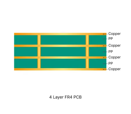
4 Layer FR4 PCB Production Record #FR4-20260402-041
| Parameter | Value | Parameter | Value |
|---|---|---|---|
| PCB Type | FR4 PCB | Quantity | 100 pcs |
| Layers | 4 Layers | Board Type | Panel PCB |
| Dimensions | 33.91 x 84.52 mm | Copper Weight | 2oz |
| Thickness | 1 mm | Min Track / Spacing | 6/6mil↑ |
| Surface Finish | ENIG (Immersion Gold) | Min Hole Size | 0.3mm↑ |
| Solder Mask | Black | Silkscreen | White |
| Stack-up | Default | Impedance Control | No |
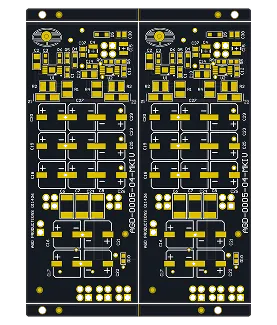
This 4-layer FR-4 PCB production run involved 100 pieces (50 sets) of 1.0mm thick boards measuring 33.91 × 84.52 mm, built with TG170 material and 2oz copper on both inner and outer layers. The design specified 6 mil minimum trace/space, 0.3 mm minimum hole size, black solder mask, white silkscreen, and ENIG surface finish. All vias required resin plugging, with final panelization in 2×1 format plus 4 mm process edges on top and bottom, yielding an overall panel size of 67.56 × 92.46 mm. 100% flying probe testing was performed prior to mechanical forming and shipment.
During DFM review, several engineering issues required resolution. Stackup structure provided by the customer was adjusted to align with our standard high-TG FR-4 build practices for reliable interlayer registration and copper balance. Panelization dimensions in the fabrication notes did not match the actual 2×1 array calculation, which was confirmed and corrected before tooling. Multiple silkscreen characters overlapped solder mask openings and via pads; these were removed after customer approval to prevent ink contamination during assembly. Solder mask openings on certain pads were also optimized to eliminate exposed copper risks around the perimeter. Resin plugging specifications for 8 mil vias were implemented after Gerber verification, ensuring reliable via protection.
All adjustments were documented and approved prior to production release. The order completed within the 15-day lead time with consistent thickness control, proper ENIG deposition, and full electrical compliance. For details on the stackup adjustment and panelization verification performed on this build, refer to the corresponding engineering case study.
Standard multilayer solution offering practical routing density and controlled impedance for industrial and consumer electronics.

In-depth guide to the most frequent Engineering Queries (EQ) and DFM issues in Multilayer FR4 PCB (4/6/8+ layers) production. Real factory insights on stack-up confirmation, impedance control, copper balance, inner layer design, via treatment, registration, and practical prevention strategies.
| Order ID | PCB Type | Layers | Dimensions | Solder Mask | Surface Finish | Quantity | Action |
|---|---|---|---|---|---|---|---|
| FR4-20260630-014 | FR4 PCB | 2 | 126 x 145 | Green | ENIG (Immersion Gold) | 10 | View detail |
| FR4-20260605-042 | FR4 PCB | 4 | 65 x 100 | Green | HASL Lead Free | 5 | View detail |
| FR4-20260605-041 | FR4 PCB | 4 | 66.04 x 54.1 | Green | HASL Lead Free | 5 | View detail |


