










This 2-layer FR-4 order with 3 oz copper on one side presented several manufacturability hurdles during CAM review. At 245.59 × 304.79 mm and 1.6 mm thickness, the board combined standard features with tight mechanical tolerances and thick copper constraints that required multiple clarifications. Large panel quantities (2800 pcs) amplified the importance of resolving these issues before production release.
Thick copper designs frequently trigger detailed engineering questions because etching and mechanical processing behaviors differ significantly from 1 oz boards. Our CAM team focused on slot dimensions, legend placement across copper/substrate boundaries, V-cut interference, and process capability limits to avoid costly production problems.
2 Layer 3oz Copper FR4 PCB Project Specifications
The order involved a 2-layer FR-4 TG150 board ( #FR4-20260611-021 ) with 1 oz / 3 oz copper weight, 1.6 mm finished thickness, and 0.3 mm minimum hole size. Solder mask was specified as cold white on top and cold red on bottom, with black silkscreen on both sides. Surface finish was lead-free HASL. The panel used 1×2 arrangement with V-scoring plus routing. The job targeted 2800 pieces (1400 sets) with an 11-day lead time and engineering test requirements.
Although the layer count was low, the combination of thick copper, narrow slots, and specific mechanical tolerances created several DFM conflicts that needed resolution before releasing the data to production.
Tight Slot Tolerances and Narrow Openings on 3oz Copper
One of the most critical issues involved slot holes with customer-specified tolerances of ±0.05 mm. Our process capability for thick copper boards typically requires wider tolerances (±0.1 mm width and ±0.127 mm length) to account for etching undercut and mechanical routing variation. Additionally, some designed slot widths were only 0.2 mm, which falls below reliable fabrication limits for 3 oz copper PCB.
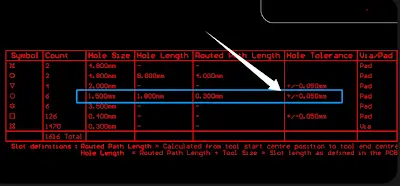
Figure 1: the tolerance for the slot hole at the arrowed location
We noticed these constraints while comparing the drill/routing files against our equipment capabilities. Our engineer recommended relaxing the tolerances to achievable levels while maintaining functional requirements. If ignored, the slots could suffer from incomplete milling, rough edges, or dimensional deviation, leading to assembly fit issues or stress concentrations that cause board warpage or delamination during thermal cycling.
In thick copper etching, narrow features are particularly prone to over-etching or under-etching, resulting in open circuits or weakened mechanical strength. This case reinforced why we always verify mechanical feature tolerances against actual manufacturing data.
Thick Copper Narrow Void Fabrication Challenge
A notable EQ highlighted narrow voids (similar to those shown in the provided reference images) with a designed width of only 0.2 mm on this thick copper board. Our CAM engineer flagged this immediately because features this narrow on 3 oz copper are extremely difficult to etch reliably and often fall outside standard process capabilities.
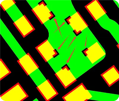
Figure 2: voids similar to those shown in the picture cannot be achieved because the designed width is only 0.2mm
We noticed that achieving such fine openings would risk severe undercutting, incomplete removal of copper, or ragged edges that compromise both mechanical and electrical integrity. After internal review, we confirmed with the customer that these voids needed widening to a manufacturable minimum. Our suggestion was to adjust the design to at least 0.3–0.4 mm depending on the specific location and function.
If this issue had been ignored and production continued with the original 0.2 mm design, the voids could result in residual copper causing shorts, irregular etching leading to signal instability, or mechanical weakness that might cause cracking under thermal expansion. In thick copper processing, these narrow features are particularly prone to yield loss and scrap, especially in a high-volume run of 2800 pieces.
Silkscreen Legend Placement on Copper vs Substrate Boundaries
Several characters on the board were positioned half on copper foil and half on substrate material. This mixed placement would likely cause the legend to appear broken or incomplete after printing and curing.
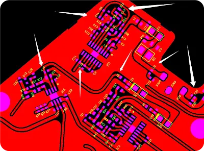
Figure 3: some characters on the board are partially placed on the copper foil and partially on the substrate
Our CAM team identified this during silkscreen layer review. We confirmed with the customer and suggested repositioning or adjusting the legend to sit entirely on one surface type. Proceeding without correction would have produced blurry or fractured characters, leading to cosmetic rejection or readability problems during quality inspection and field use. According to common IPC-A-600 criteria, such defects can fail acceptability standards for marking legibility.
V-Cut Interference and Depanelization Conflicts
Components or features were located directly on V-cut lines in the panel data. Additionally, there was inconsistency between the requested V-cut + bridge method and the presence of stamp holes in the production files. Our engineer pointed out that parts on the scoring line would be damaged or severed during depanelization.
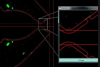
Figure 4: V-cut+connecting tab+stamp hole
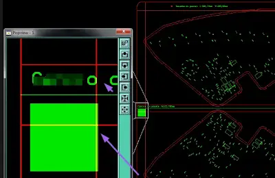
Figure 5: the arrow part text was designed on the V-cut line
We recommended shifting features away from scoring paths and standardizing the depanelization approach. If left unaddressed, this would result in scrap boards, damaged components, or rough edges that complicate downstream assembly. In high-volume runs like 2800 pieces, such errors multiply quickly into significant yield loss.
Solder Mask Thickness, Ink Color Availability, and Drill Data Inconsistencies
The specified solder mask thickness was non-standard, making process control difficult. The customer requested cold white ink, which was unavailable in our standard inventory. Drill layer hole counts also did not match the provided hole chart. Small character sizes in the legend exceeded our minimum line width capability, risking blurred or unreadable markings.
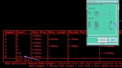
Figure 6: the number of holes in thedrill map does not match the number of drilling layers
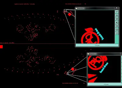
Figure 7: these highlighted characters are too small in height and width
We confirmed alternative ink options and adjusted mask parameters within controllable ranges. These adjustments prevented registration issues and ensured consistent coverage. Without clarification, non-standard mask thickness could cause uneven coverage, leading to exposed copper or poor insulation, while mismatched drill data might result in missing or extra holes.
DFM Risks for Thick 3oz Copper 2 Layer FR4 Boards
Heavy copper boards demand greater attention to etching compensation and mechanical feature sizing. Designers often apply tolerances suitable for thin copper without accounting for increased etch factor and plating dynamics. Narrow slots and tight mechanical tolerances are among the most common triggers for EQs on such designs, frequently leading to production delays if not resolved early.
Legend placement across dissimilar surfaces and V-cut conflicts further illustrate how small oversights in data preparation can cause major downstream problems, including scrap, rework, and repeated engineering cycles. These issues highlight the gap between design tools and actual factory process windows.
| Issue | Cause | Resolution |
|---|---|---|
| Slot Tolerances | ±0.05mm on 3oz copper | Relaxed to process capability |
| Legend Placement | Cross copper/substrate | Repositioned to single surface |
| V-Cut Interference | Features on scoring lines | Shifted features and standardized method |
| Mask & Drill Data | Non-standard specs and mismatches | Adjusted parameters and confirmed alternatives |
Table 1: Main DFM Issues in 3oz Copper 2 Layer PCB. These changes supported reliable high-volume production.
Resolution of Thick Copper DFM Issues
Our team worked through each point systematically. Slot tolerances were adjusted to manufacturable values, legend elements repositioned, and V-cut paths cleared of interfering features. We standardized the depanelization method after confirming customer preference and updated drill files for consistency. Ink alternatives and mask parameters were finalized within our process capability.
To reduce manufacturing risk, our engineer adjusted copper clearances and routing compensation for the 3 oz layer. This helped maintain feature integrity and prevented potential copper peeling or incomplete etching that could have occurred with the original tight parameters.
Production Release Outcome
After receiving all necessary customer confirmations, the CAM data was optimized and approved. Panelization, mechanical features, and surface layers were aligned with production realities. The order was released for fabrication with improved first-pass success potential.
DFM Best Practices for 3oz Copper 2 Layer FR4 Designs
- Verify mechanical slot and cutout dimensions against your fabricator's thick copper process capabilities before finalizing tolerances.
- Avoid placing silkscreen legends across copper-to-substrate boundaries to prevent broken or blurred characters.
- Keep critical features clear of V-cut or scoring lines in panelized designs.
- Confirm special ink colors and mask thicknesses early, as availability varies by factory.
- Ensure drill files, hole charts, and outline data are fully consistent across all layers.
- Apply appropriate etching compensation and annular ring considerations for thick copper layers.
- Provide clear fabrication notes for depanelization methods when mixing V-scoring, routing, and stamp holes.
FAQ
Q1: Why are tight tolerances problematic on thick copper slots?
A1: Thick copper etching behaves differently and requires more compensation. Extremely tight tolerances often exceed process capability, leading to dimensional inaccuracies or incomplete feature formation.
Q2: What happens when silkscreen crosses copper and substrate areas?
A2: Ink adhesion and curing differ between surfaces, causing characters to crack, blur, or detach, resulting in legibility failures during inspection.
Q3: Why must features be kept away from V-cut lines?
A3: Scoring cuts into the board; any components or copper on the line will be damaged or severed, causing immediate scrap or assembly issues.
Q4: How do drill data inconsistencies affect production?
A4: Mismatched hole counts can lead to missing holes, extra drilling, or program errors that compromise board functionality and require full re-fabrication.
Q5: Why is non-standard solder mask thickness a concern?
A5: It complicates thickness control and registration, increasing risks of thin spots, exposed copper, or poor insulation performance.






