










PCB Specifications
| Parameter | Value | Parameter | Value |
|---|---|---|---|
| PCB Type | FR4 PCB | Quantity | 1400 pcs |
| Layers | 2 Layers | Board Type | Panel PCB |
| Dimensions | 245.59 x 304.79 mm | Copper Weight | 3oz |
| Thickness | 1.6 mm | Min Track / Spacing | 6/6mil↑ |
| Surface Finish | HASL Lead Free | Min Hole Size | 0.3mm↑ |
| Solder Mask | White | Silkscreen | Black |
| Stack-up | Custom | Impedance Control | No |
Manufacturing Timeline
Logistics Information
Key Manufacturing Processes
Manufacturing Summary
This 2-layer FR-4 board measures 245.59 × 304.79 mm with 1.6 mm thickness, TG150 material, and asymmetric copper weights of 1 oz inner/3 oz outer. Produced as 1×2 panels for a total of 2800 pieces using lead-free HASL surface finish, the order featured 0.3 mm minimum holes and 6 mil line/space. V-cut combined with routing defined the final separation, with black silkscreen and cold white solder mask applied over the heavier copper side.
DFM review addressed multiple manufacturability concerns. Narrow 0.2 mm slots in the thick copper area were impossible to produce reliably and required confirmation of adjusted dimensions. Silkscreen characters positioned half on copper and half on substrate risked breakage, while extremely small highlighted characters exceeded process capability for clear readability. Drill layer counts did not match the provided hole data, V-cut lines intersected critical features, and non-standard solder mask thickness needed agreement for process control. Tolerance adjustments on slots and stamp hole configurations were also aligned before release.
All clarifications were resolved prior to production, allowing consistent execution of the heavy copper PCB layout and HASL thickness consistency across the large batch. Engineering test fixtures verified electrical performance, and the full quantity shipped within the 11-day window with complete test reports and quality documentation. Final boards met dimensional and functional requirements with no impact from the resolved DFM points.
Explore More PCB Manufacturing Resources
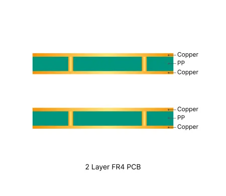
2 Layer FR4 PCB Manufacturing Insights
2 layer FR4 PCBs deliver cost-effective solutions for most electronic designs. Their simple structure enables consistent quality and efficient production cycles.
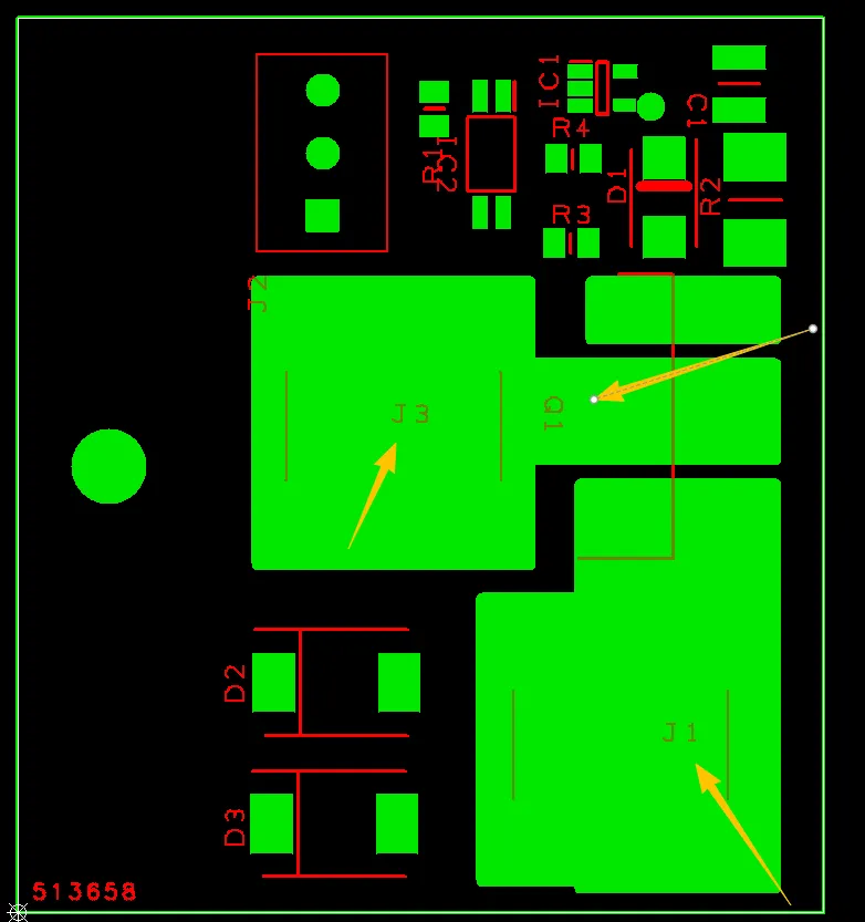
Common Engineering Queries in 2 Layer FR4 PCB Design and Manufacturing
Real Engineering Queries (EQ) and DFM issues for 2 Layer FR4 PCB (double-sided boards) from actual production reviews. Learn how to avoid common problems with via treatment, silkscreen on pads, solder mask openings, hole attributes, board edge clearance, and other frequent design pitfalls.
Real Production Records
| Order ID | PCB Type | Layers | Dimensions | Solder Mask | Surface Finish | Quantity | Action |
|---|---|---|---|---|---|---|---|
| FR4-20260905-007 | FR4 PCB | 2 | 42.8 x 38.8 | Green | HASL Lead Free | 5 | View detail |
| FR4-20260904-029 | FR4 PCB | 2 | 14 x 18 | Black | HASL Lead Free | 125 | View detail |
| FR4-20260831-062 | FR4 PCB | 2 | 103.65 x 115.06 | Green | HASL Lead Free | 5 | View detail |


