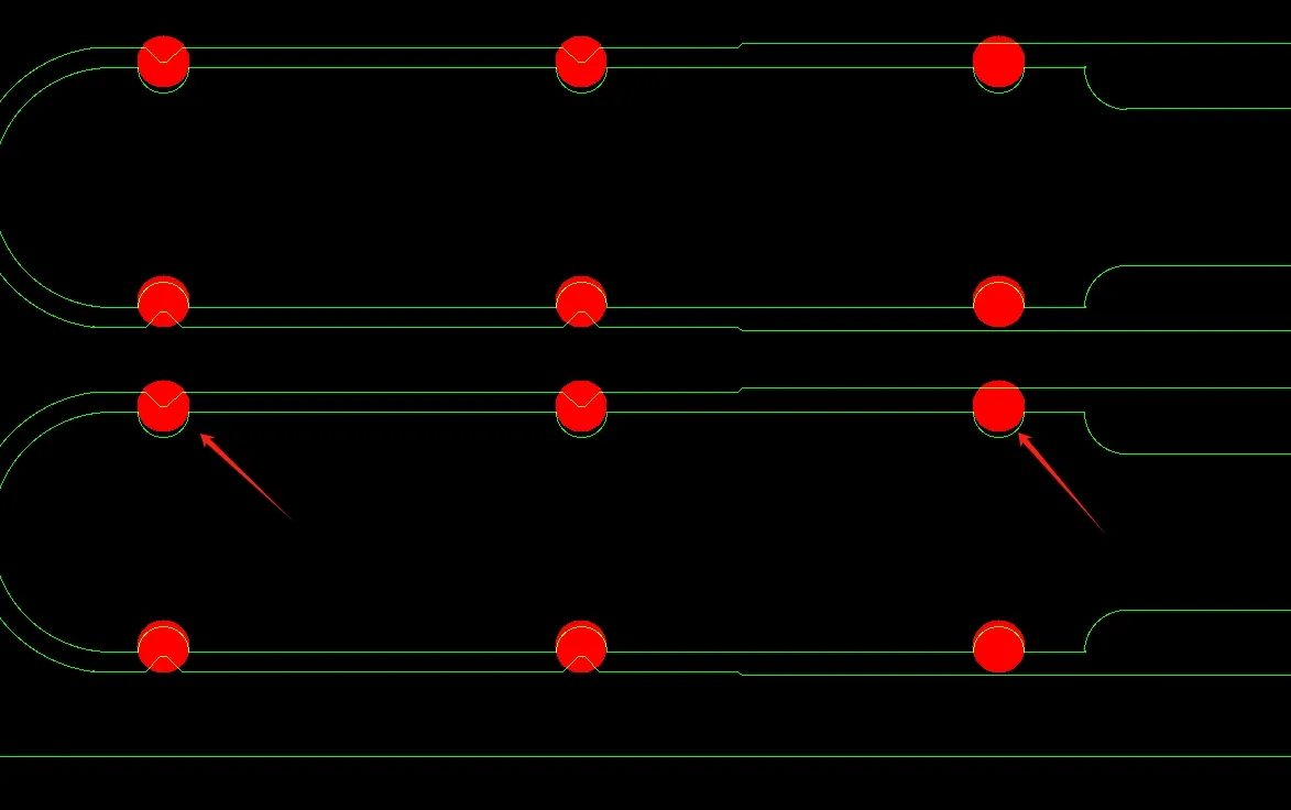
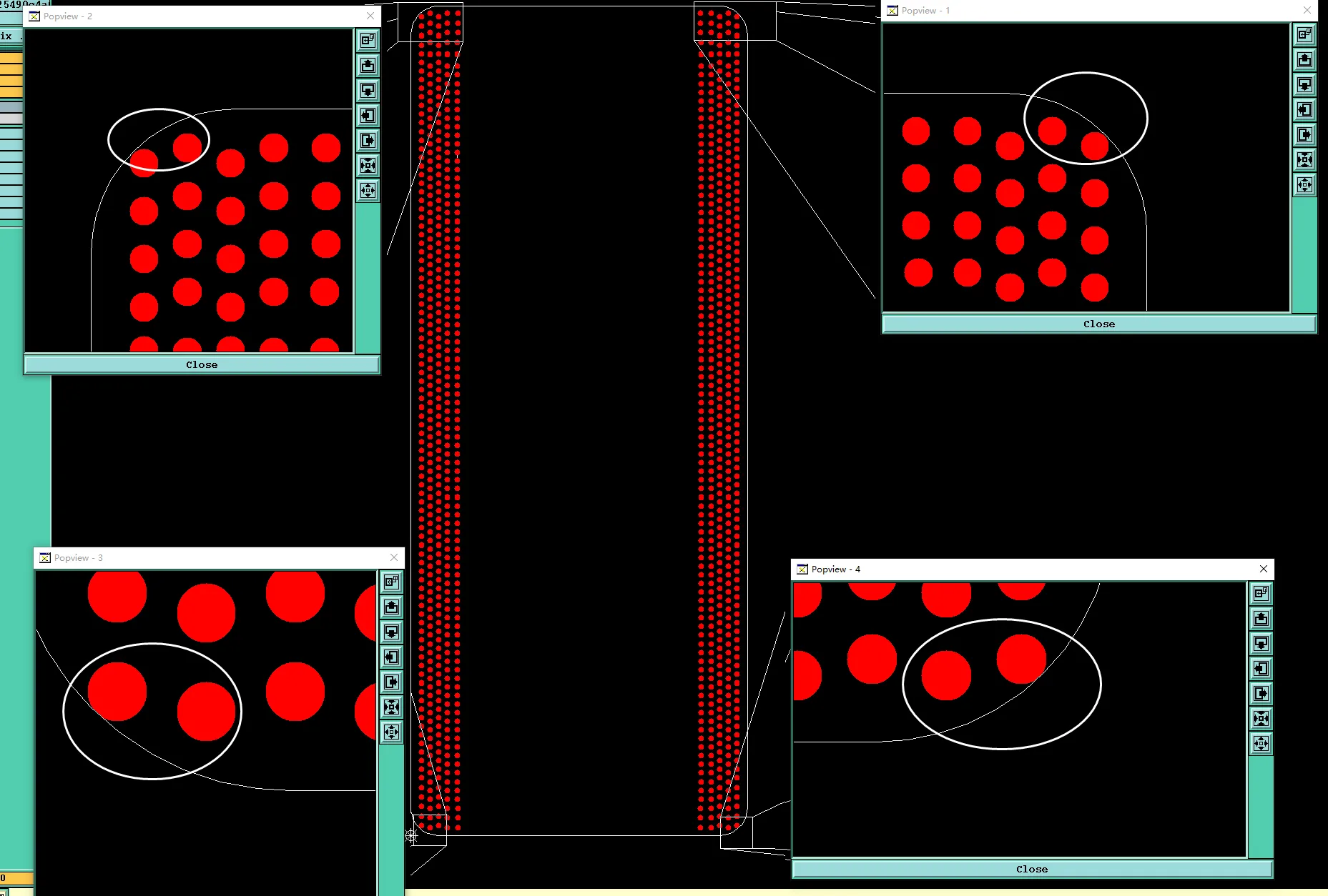
CAM review of a 62.7 × 62.7 mm 6-layer FR-4 PCB order revealed a significant NPTH hole with pad conflict. The drill file designated specific holes as NPTH, yet copper pads appeared on both outer layers in the Gerber data. This inconsistency halted production pending clarification, as it directly affected plating sequences, annular ring integrity, and overall manufacturability for the 20-piece (5-set) 2x2 panel run.
With 1.6 mm finished thickness, 1 oz copper, ENIG surface finish, and standard TG170 material, precise hole processing was non-negotiable. Our engineering investigation focused on resolving this NPTH vs PTH hole attribute confirmation challenge to align customer design intent with factory execution.
Compact 6-Layer Board Mechanical and Electrical Requirements
The project ( #FR4-20260318-061 ) specified a square outline board using FR-4 base material, 6 layers, and 0.2 mm minimum hole size. Fabrication parameters included immersion gold finishing, 100% flying probe testing, and mechanical forming. Panelization followed a 2x2 array with 5 mm process margins on all sides to support efficient production of the 20 pieces.
Design files indicated non-plated through holes for mechanical purposes such as mounting or alignment. However, the presence of defined pads suggested additional considerations for component interface or structural reinforcement. This setup required careful interpretation to maintain both mechanical stability and electrical isolation where intended, particularly around the highlighted hole positions.
Drill File NPTH Designation vs Gerber Pad Features
During initial data import, our CAM team observed a clear mismatch. Holes explicitly tagged as NPTH in the drill output showed corresponding annular rings and copper pads on top and bottom layers. This non-plated hole with copper pads PCB configuration raised immediate flags regarding processing order and final attributes.
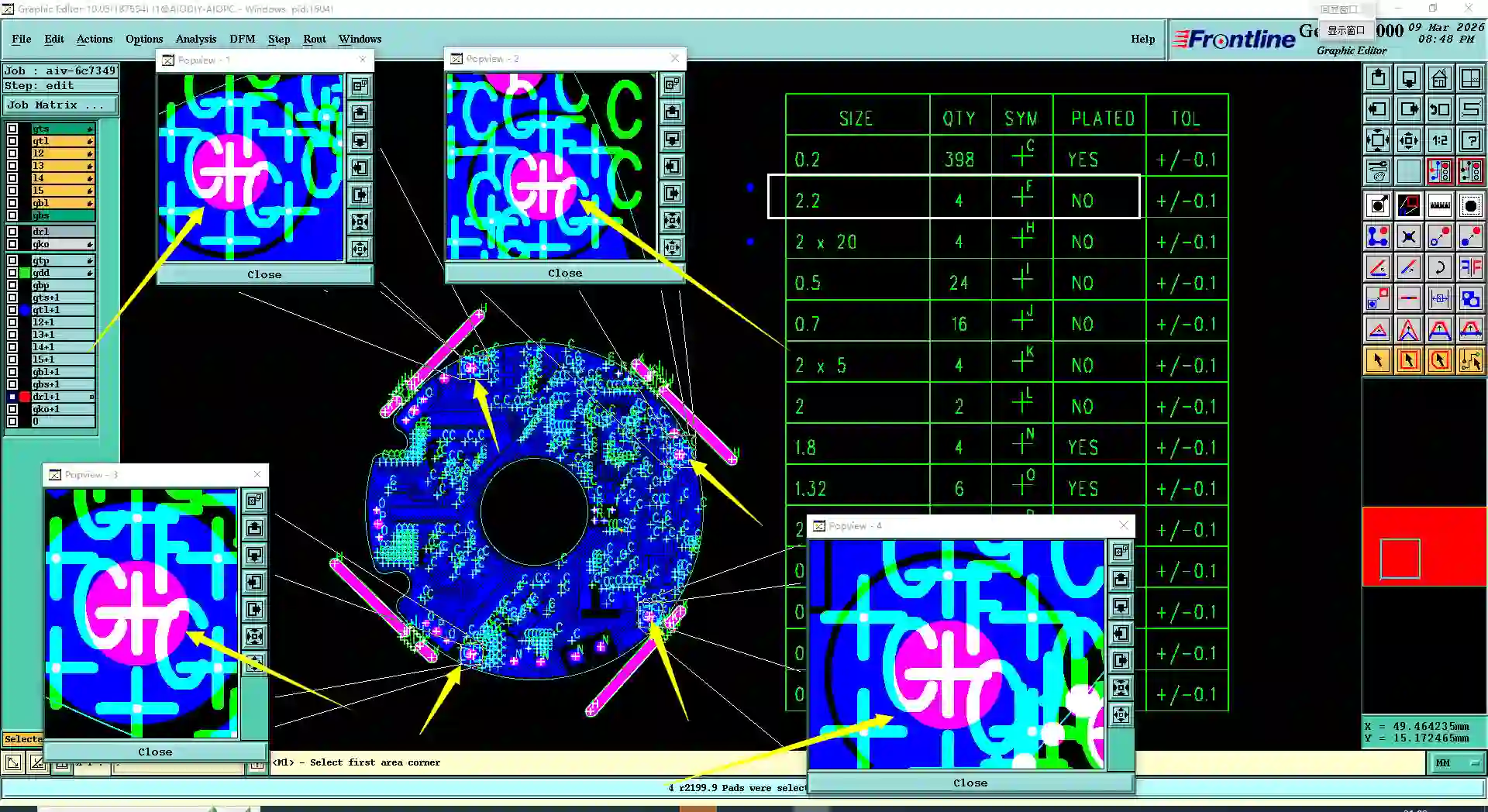
Figure 1: the Non-plated Through holes (NPTH) in the drill file have pads on both sides
Our CAM engineer noted the potential for misprocessing: plating the holes would contradict the NPTH definition, while skipping plating might leave pads without proper support or isolation. The 18 μm copper thickness and board dimensions amplified the importance of accurate classification to avoid tolerance stack-up issues in the compact layout.
| Data Source | Specification | Observed Conflict |
|---|---|---|
| Drill File | NPTH Attribute | Post-plating drilling expected |
| Gerber Layers | Pads on Both Sides | Annular ring implies possible PTH intent |
| Fabrication Notes | No explicit hole handling | Ambiguous manufacturing path |
Manufacturing Risks from Unresolved Hole Attribute Mismatch
The primary risk involved incorrect sequencing in the production line. Treating the feature as PTH would deposit copper in the barrel, potentially creating unintended conductivity. Processing strictly as NPTH risked pad delamination or insufficient mechanical strength under component stress, especially critical for a 1.6 mm thick board undergoing ENIG finishing.
IPC-6012 guidelines emphasize consistent hole definitions to ensure Class 2 reliability. Ambiguity here could lead to electrical test failures, rework, or field issues like intermittent connections around mechanical fixation points. The 2x2 panel setup further magnified risks, as a single misprocessed hole type could affect multiple boards per set.
Additional file elements, including English image notes (to be ignored per standard process) and GBL layer copper clearance, supported the need for full verification but remained secondary to the core NPTH hole with pad issue.
Panel Orientation and Documentation Gaps in Production Data
Supporting the main investigation, panel diagram confirmation was requested to prevent orientation errors on the square board. Limited large copper clearance areas on inner layers also prompted review to ensure proper pad isolation near the disputed holes. These elements reinforced the overall documentation consistency challenges typical in such orders.
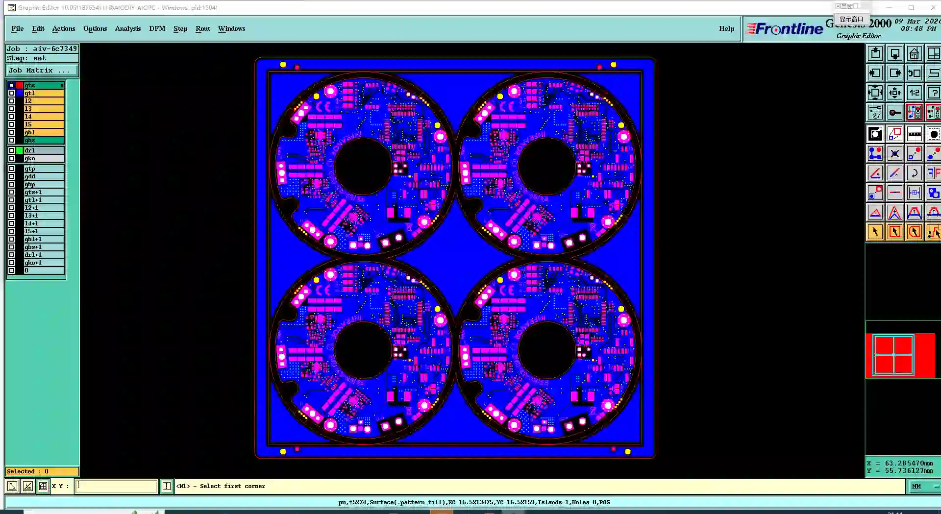
Figure 2: panel diagram confirmation
EQ Resolution Path for NPTH Pad Configuration
The Engineering Question explicitly asked for confirmation on the highlighted hole: NPTH as per drill data despite bilateral pads. Customer clarification confirmed mechanical NPTH intent with pads for surface mounting support only. No barrel plating was required.
We updated drill programs for post-plating execution, verified panelization orientation, and aligned all image notes to conventional factory processes. Revised manufacturing files ensured the ENIG-finished boards met electrical and mechanical specifications. Production release followed successful internal validation.
| Before Clarification | After Resolution |
|---|---|
| Ambiguous hole type risking plating error | Confirmed NPTH with surface pads only |
| Unverified panel orientation | Locked 2x2 diagram |
| Potential test or assembly defects | Ready for reliable production |
Practical Guidelines to Prevent Hole Plating Interpretation Errors
- Clearly annotate all NPTH features with pads in both drill legends and fabrication notes to support accurate PCB hole type definition error prevention.
- Provide cross-referenced layer views showing intended pad functionality for non-plated through hole with annular ring designs.
- Use dedicated mechanical hole symbols distinct from vias in CAD output to aid CAM review.
- Validate copper-to-hole relationships early, especially in dense 6-layer layouts, referencing IPC spacing principles.
- Include panelization intent diagrams with orientation markers for symmetric boards.
- Consolidate special instructions in standard text notes rather than image-only remarks.
- Perform pre-submission DFM simulations focusing on plating boundaries and drill attributes.
- Engage manufacturers proactively on any hybrid hole features during design finalization.
Conclusion
Resolving the NPTH hole with pad ambiguity through targeted EQ ensured this 6-layer order advanced without compromise. The case underscores how detailed CAM analysis bridges minor data discrepancies into robust production outcomes, safeguarding quality for FR-4 multilayer projects.
FAQ
Q1: What causes NPTH hole with pad conflicts during PCB CAM review?
A1: Mismatches between drill file attributes and Gerber copper features create uncertainty about plating requirements, triggering clarification to prevent processing errors.
Q2: How do NPTH pads affect manufacturing for multilayer boards?
A2: They require confirmed post-plating drilling to preserve pads without barrel copper, maintaining mechanical strength and electrical isolation as designed.
Q3: Why confirm panel diagrams alongside hole attribute questions?
A3: Square boards risk rotation errors in multi-set panels, which could misalign critical NPTH features and compound attribute issues.
Q4: What IPC standards guide NPTH vs PTH hole attribute confirmation?
A4: IPC-6012 and IPC-A-600 provide criteria for hole quality, plating, and annular rings, supporting consistent interpretation across data sets.
Q5: Can designers avoid PCB manufacturing hole attribute clarification delays?
A5: Yes, by using explicit, multi-file documentation and early DFM reviews focused on hybrid hole features like non-plated holes with pads.
Q6: What happens if NPTH pad intent remains ambiguous?
A6: Production pauses for EQ, potentially causing schedule slips, or risks defects if processed incorrectly, affecting reliability in assembly and operation.