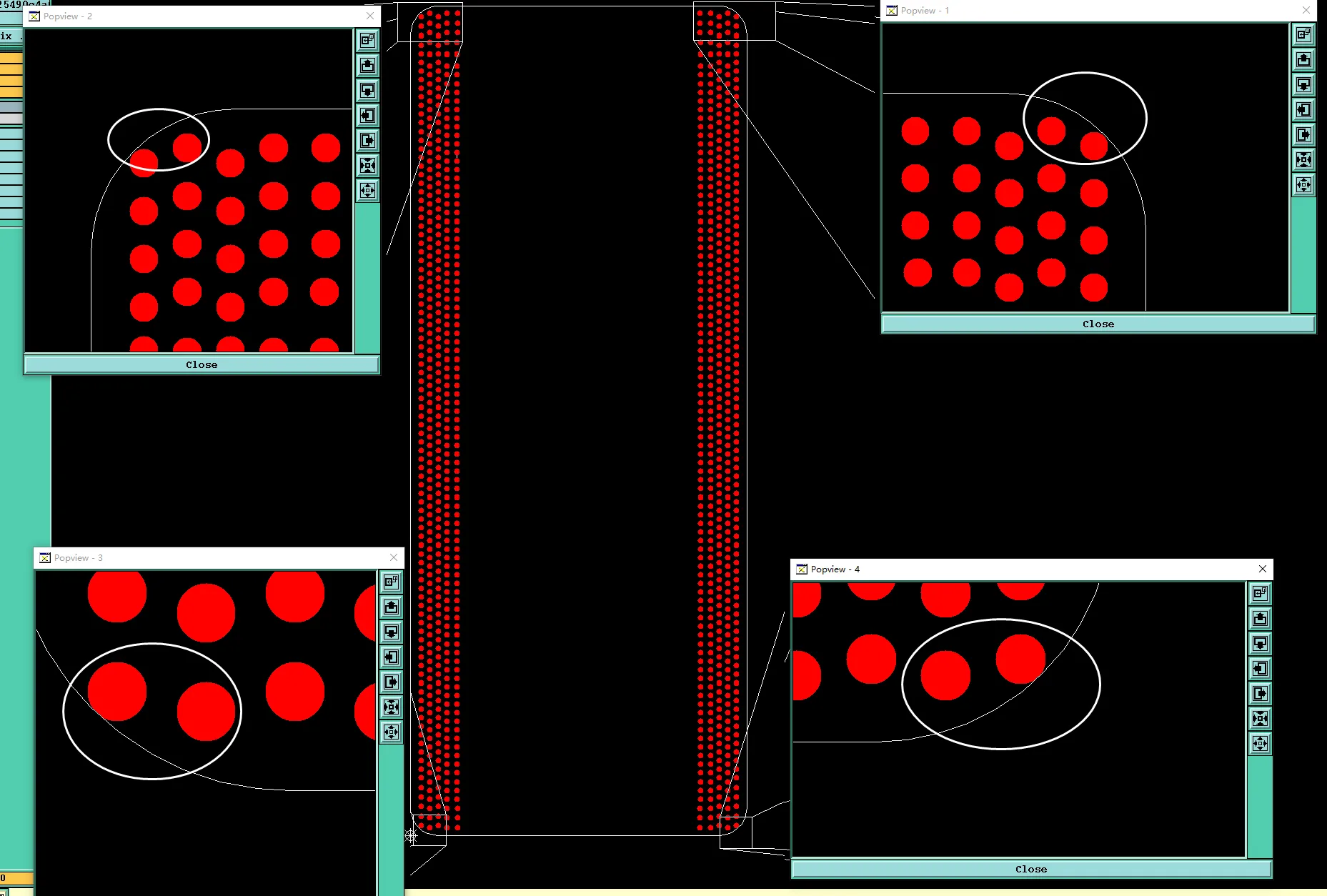
PCB UL marking can be required in the fabrication drawing or order even when the released silkscreen Gerber does not contain the required marks.
For CAM, the issue is not simply whether there is empty space on the board. The review has to separate what the drawing requires, what the Gerber already contains, who owns each marking, and whether the released PCB construction can carry the requested UL marking.
This becomes an EQ when the drawing calls for manufacturer identification, a UL mark, or a date code, but the silk file does not define the corresponding artwork—or when the marking request is paired with a laminate and solder mask color that the factory cannot apply UL marking to as released.
The same review logic also applies when a silkscreen block appears in the Gerber but the package contains no QR-code instruction.
| What the package released | What production proposed | What still has to be confirmed |
|---|---|---|
| Drawing requires manufacturer identification, UL marking, and date code; silk at the site is empty or incomplete | Factory identification, a UL set, and a date-code site added on top silkscreen at the drawing location | Side, coordinates, and the UL element list. A completed add is still a proposal. |
| Note lists marking, date code, lot number, and serial number; stackup names a laminate and solder mask color | This construction is not in the factory UL recognition | Whether UL marking stays, drops, or the construction changes. Date code, lot, and serial number stay on their own rows. |
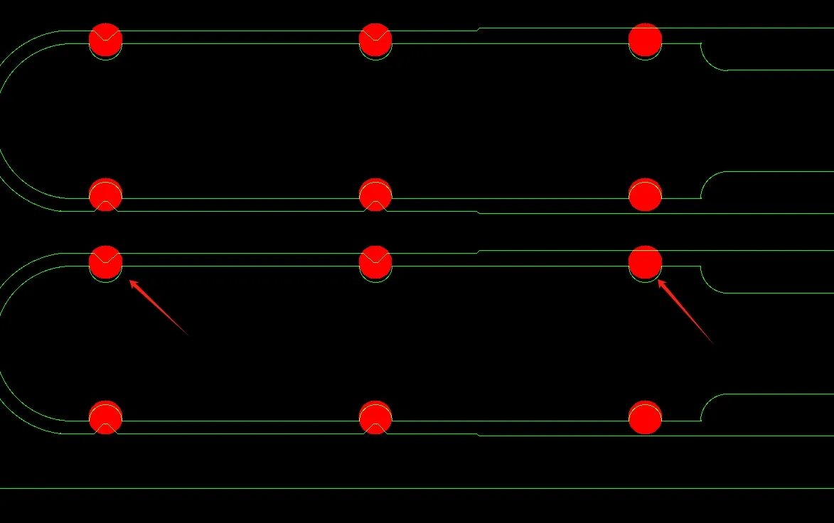
| Silkscreen contains a filled block; notes have no QR requirement | Control the flash as a conventional silkscreen block | Whether the block is only legend, and whether the drawing reserved that site for factory identification or date code |
PCB Marking Requirements: Drawing vs. Silkscreen Layer
PCB marking requirements live in the fabrication drawing and the order. Those documents state required versus not required for manufacturer identification, UL marking, date code, lot number, and serial number. They also state side and approximate site when the note includes them.
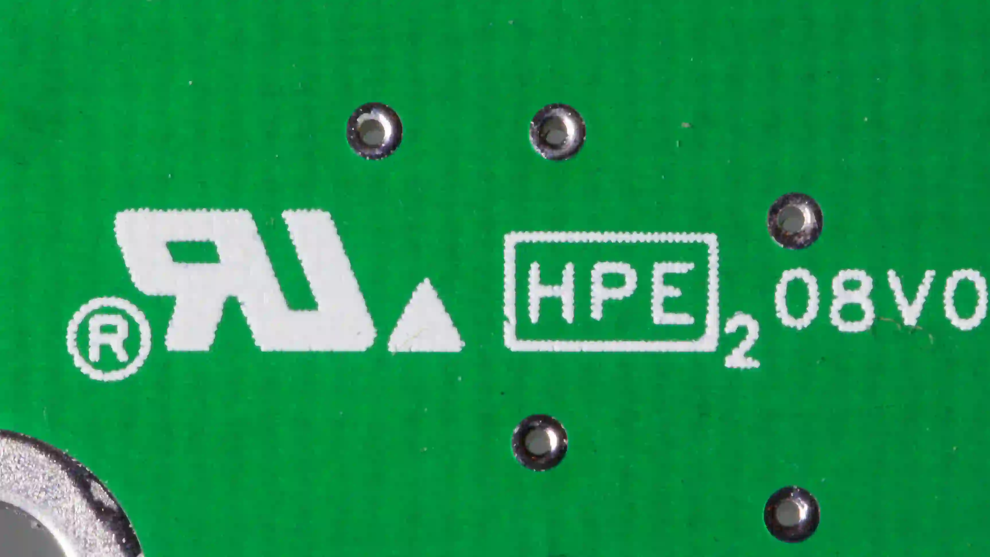
The Gerber silkscreen layer holds printable geometry. An empty site, a reserved box, or a customer logo does not stand in for the factory UL set. This is a common PCB silkscreen and marking consideration in CAM review. In the file list that layer is usually GTO or GBO. The flashes there are legend. They do not, by themselves, establish recognition or specify a QR code.
Overlay of silk to outer copper, and of the drawing dimension to the silk site, can show occupancy. The site may be empty, boxed, already lettered, on the opposite side from the dimension, or sitting on a land or on copper. Occupancy answers those questions. It does not answer recognition of this laminate and this solder mask color, the legal UL element list when the note only says "UL," a date-code format the package never wrote, a lot or serial-number rule, or a payload inside a filled rectangle.
A filled silkscreen block is still legend geometry until a note names a code.
| Source | What it can identify | What it leaves open |
|---|---|---|
| Fabrication drawing / order note | Required versus not required; named identifiers; side and site if the note states them | Recognition of this laminate and solder mask color; the UL element list behind the word "UL"; a date-code format that was never written; QR payload or data owner |
| Gerber silkscreen layer | Occupancy: empty, boxed, already lettered, wrong side, on a land or on copper | Whether a drawn logo is recognized UL marking; whether a rectangle is a QR specification |
| Stackup / material callout / order color | Laminate system and solder mask color as released | Whether another plant's recognition applies to this job |
| Silk-to-copper overlay | A block sitting on a land or trace; a side mismatch against a dimensioned site | Whether factory identity may be added at that site |
Tag each identifier before silk is edited: customer-drawn, factory-added, or missing. Record occupancy on its own line. Reading a drawing sentence and converting it into artwork in the same pass leaves the row open.
Factory ID, UL Logo, and Date Code Added on Top Silkscreen
The drawing asked for three objects that the silk file does not contain: manufacturer identification, a UL logo or mark set, and a date code. Production then placed its identification, a UL set, and a date-code site on the top silkscreen at the drawing location and asked for confirmation. This type of PCB engineering review requires the production-added markings to be checked against the released drawing rather than assumed to be part of the original silk data.
"Full UL" is an open list until the customer names the elements: the mark device, the UL file number, a type designation, or some combination of them. A customer line that only says UL, or that uses wording such as "factory code," does not yet tell production which of those objects belong on the board.
Date code is production-variable. The drawing can reserve a site. It does not pre-print the week string. A format belongs in the instruction when the package states one. A request for week-year is a format only when that string is actually in the note.
A drawing dimension with no side, followed by an add on top silk, still leaves side open. Top is a proposal, not a reading of the drawing.
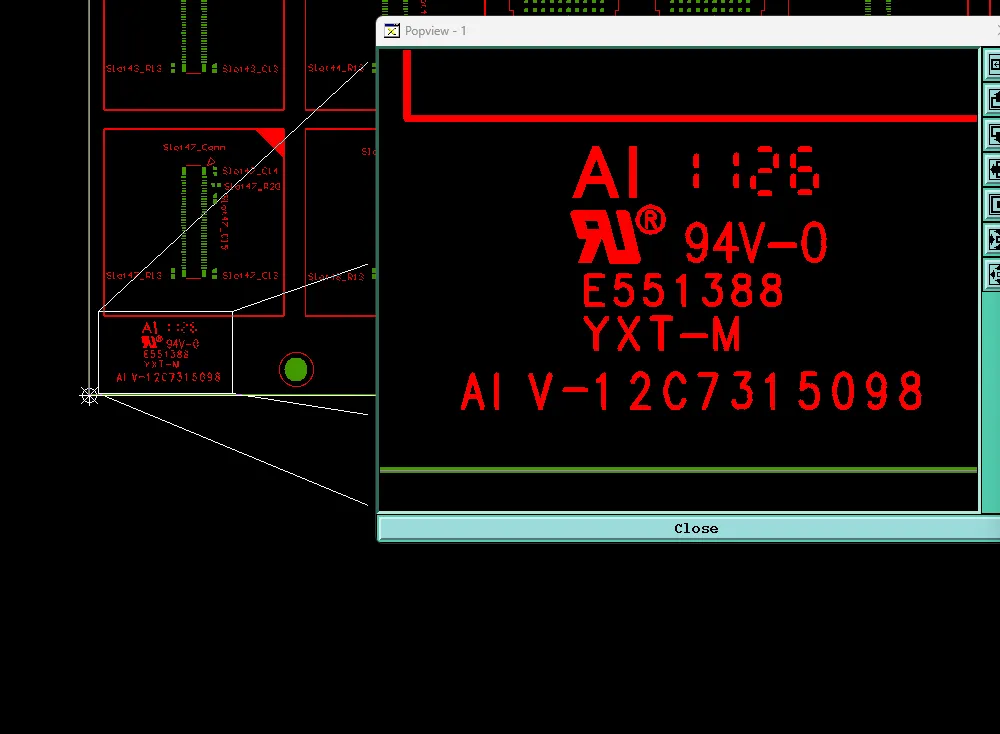
Adding our factory code, full UL markings, and the year mark to the top-layer silkscreen at the location shown in the drawing.
An empty printable site does not, by itself, authorize a change to board identity. A factory add of UL marking is a proposal until the close names author, element list, side, and coordinates.
Laminate and Solder Mask Color With No UL Recognition
UL marking follows this factory's recognition for a construction. For PCB silkscreen marking CAM review, the laminate system and solder mask specification are key construction inputs when checking whether the requested UL marking can be applied to the released build. Color sits inside that construction, not as a cosmetic field next to the logo.
A note can list marking, date code, lot number, and serial number in one line. Recognition attaches to UL marking. It does not attach to date code, lot number, or serial number. Moving a PCB UL logo, or adding lot and serial number, does not create recognition. A logo in silkscreen is artwork. It is not the construction file.
Read laminate and solder mask color from the drawing, the stackup, and the order — not from silk. The question on this row is whether this construction may carry UL marking.

Our company does not hold UL certification for this type of board material and solder mask color.
The usual closes stay inside that question: change laminate and/or solder mask color to a recognized construction, drop UL marking, or run the job where that construction is recognized. This article does not list ratings or file numbers.
Date code, lot number, and serial number stay on their own rows. Dropping the UL mark does not, by itself, remove those identifiers. Four identifiers, four answers.
PCB QR Code Marking: When a Silkscreen Block Is Not a QR Code
Silk contains a block. The package has no QR, 2D, or barcode note, no payload, and no data owner. Customer wording on that flash is sometimes "white oil." The geometry is still a silkscreen block.
The usual proposal is to leave the flash as conventional silkscreen rather than generate a code from the rectangle.
A later request for PCB QR code marking needs a payload or a generation rule, static versus serialized, a site, and a process. A filled box does not carry those fields. If the flash is already a drawn matrix, say so. If it is only a solid or framed block, treat it as legend.
Manufacturer identification or date code belongs in that block when the drawing named that site for those marks. Otherwise the block and the UL row stay separate. Closing one does not close the other.
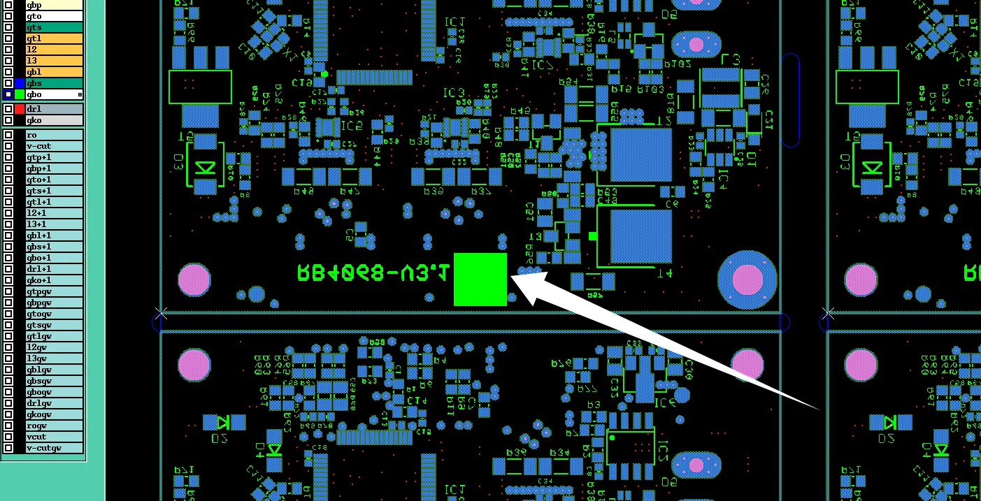
As shown, since there is no requirement to add a QR code on the white silkscreen block indicated by the arrow, it will be managed as a standard white silkscreen block.
PCB Identification Marking: Three Ways to Close the CAM EQ
One path per identifier population. UL marking and a silk block close on different rows.
| Path | When it fits | What gets recorded |
|---|---|---|
| A — Factory adds the named marks at the confirmed site | Drawing or order requires manufacturer identification, UL marking, and/or date code; site and side agreed; if UL marking is in the set, this construction is recognized | Author = factory add; the element list the customer named; site and side; recognition for this laminate and solder mask color. Lot and serial number join when they are required and a variable-data method is named. |
| B — Keep the released silkscreen; no factory UL; the block is not treated as a QR code | Customer owns all legend; UL marking is not required; the construction is unrecognized and will not change; or the block was not specified as a code | If UL marking drops, date code, lot number, and serial number still need keep or drop. The silkscreen block stays a block. |
| C — Customer revises the package | The reserved site or a static mark set needs to be drawn in Gerber; drawing notes need to match the files; laminate and/or solder mask color need to change if UL marking stays; or the block was meant to be a code | Revised silk and/or drawing. QR needs payload or owner, static versus serialized, site, and process. Recognition is re-read from the new construction, not from the new artwork. |
Path A matches the first EQ. Path B matches the second EQ when the construction will not change, and the third EQ when the block was not specified as a code. Path C is the rewrite when released silk cannot carry the required marks, or when the note and the files still disagree after the site is known.
The manufacturing instruction records author, elements, site and side, recognition, and the silk block. That record is separate from a silent edit of GTO or GBO.
What Still Has to Be Confirmed on PCB Identification Marking
Q1: Does a UL logo in silkscreen mean the board is UL recognized?
A1: A logo in the legend is artwork. Recognition is construction-specific, typically laminate plus solder mask color.
Q2: Can the factory add manufacturer identification, UL marking, and date code because the drawing asked for them?
A2: After the customer confirms the element list, the side, and the site. An empty silk site is a location, not by itself an authorization.
Q3: What does "full UL" include?
A3: Whatever the customer names: mark device, UL file number, type designation, or a combination of them. The phrase by itself is not an element list.
Q4: If this laminate and solder mask color are not recognized, do date code, lot number, and serial number come off the board?
A4: Not from that row alone. Those identifiers do not depend on UL recognition. Each one keeps or drops separately.
Q5: Is a filled silkscreen block a QR code?
A5: Not from geometry alone. With no QR note, no payload, and no data owner, the flash is handled as a conventional silkscreen block.