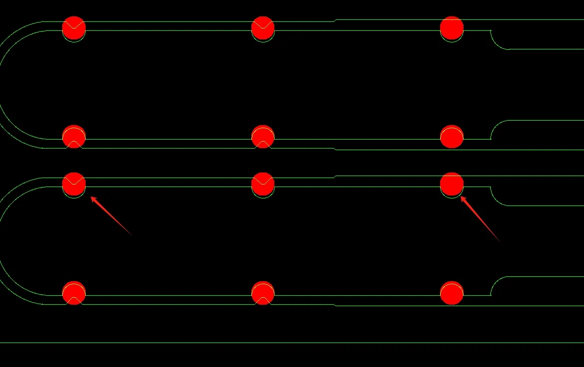
The main engineering questions recorded for this order concern minimum clearances at the board edge. The factory notes that both inner-layer and outer-layer copper approach the edge so closely that the finished board is expected to show exposed copper after outline routing. Separately, holes located around the perimeter sit close enough to the edge that the finished parts may exhibit broken holes. Both points are presented as items requiring customer confirmation. The board is a 4-layer construction using Rogers RO4003C, finished thickness 1.0 mm, copper weight 1 oz on all layers, surface finish ENIG with 2 µin gold, and no solder mask or silkscreen on either side. Outline processing is mechanical forming. Quantity is five pieces. No revised files, acceptance replies, or inspection results appear in the records.
Copper-to-Edge Clearance Issues on Rogers RO4003C PCB
The communication states that copper on both the inner and outer layers lies too near the board edge and that the finished edge will therefore expose copper. The request is simply to confirm whether this condition is acceptable. In multilayer fabrication the outline is produced by routing or punching after the layers have been laminated and the outer copper has been etched and plated. Any copper that extends into the final routed path is cut through, leaving the copper edge exposed at the perimeter. Because the board carries no solder mask, there is no additional dielectric covering that could otherwise hide or protect that edge. The absence of mask also means the exposed copper remains visible and electrically accessible once the outline is complete.
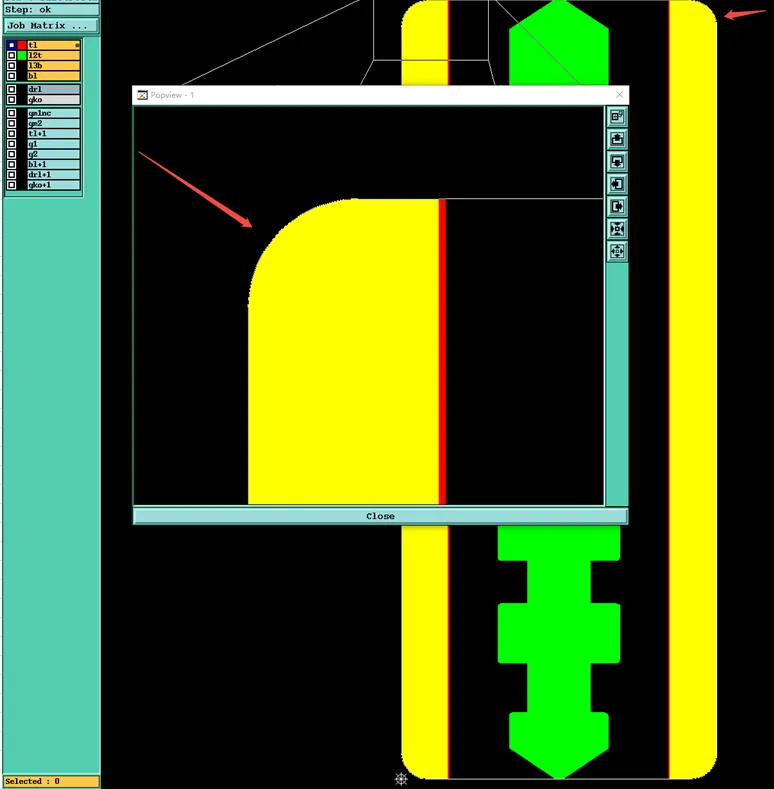
Figure 1: The copper foil is too close to the board edge
On a Rogers PCB stack the dielectric constant and loss characteristics are controlled by the laminate itself. Exposed copper at the edge does not alter those bulk properties, yet it creates a continuous conductor that terminates at the physical boundary of the board. For a high-frequency category part this geometry can matter if the exposed edge lies near a signal path or ground reference that is intended to remain internal. The records do not quantify the actual clearance distance, nor do they identify whether the copper in question is a ground plane, a power plane, or a signal trace. They record only that the distance is insufficient to keep the copper inside the finished outline and that confirmation is required.
Mechanical forming further defines the final edge location. Routing tolerances, tool wear, and panel positioning all influence how much material is removed. When copper is already designed close to the nominal outline, normal process variation can increase the length of exposed copper or, in the opposite direction, leave a narrow strip of laminate. The factory note treats the exposure as the expected outcome rather than a possible defect, and therefore seeks explicit confirmation before proceeding. No alternative copper pull-back or modified outline is proposed in the records.
Hole-to-Edge Clearance Risks During PCB Routing
The second item in the main exchange concerns holes positioned around the perimeter. The factory states that these holes lie too close to the board edge and that the finished parts may therefore show broken holes. Confirmation is again requested. Hole-to-edge clearance is evaluated after the outline is formed. If the remaining web of laminate between the hole wall and the routed edge is thinner than the process can reliably maintain, the hole wall can fracture or the hole can open to the edge during routing or subsequent handling. The records list a nominal hole diameter of 0.3 mm and note that vias are to be covered with solder mask (via-cover-oil), yet they do not specify the measured or designed clearance from hole edge to board edge.
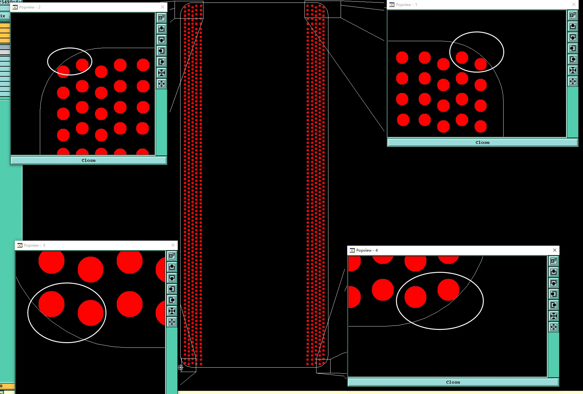
Figure 2: The holes are too close to the board edge which may lead to the broken holes on the finished PCBs
Because the outline is produced by mechanical forming, the router bit removes material from both the outer edge and, if clearance is insufficient, from the hole wall itself. On a 1.0 mm thick Rogers laminate the mechanical strength of the remaining web depends on the resin content, glass style, and the exact remaining distance. The factory note does not claim that breakage has already occurred; it states that breakage may occur and asks the customer to confirm acceptance of the risk or to authorize a design change. No proposed increase in clearance, relocation of holes, or addition of breakaway tabs is recorded.
The two clearance issues are related only in that both arise at the same stage of fabrication—the final outline operation—and both are flagged for confirmation before that operation proceeds. Copper exposure is a consequence of copper geometry intersecting the routed path; hole breakage is a consequence of hole geometry intersecting the same path. Each is documented separately, and each requires its own confirmation.
Rogers RO4003C PCB Stack-Up Thickness and Step Plating
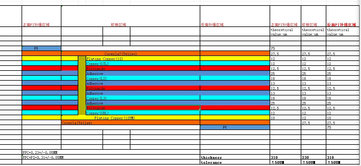
An earlier entry in the same communication asks whether the prepared stack-up and a finished edge thickness of approximately 1.1 mm ± 10 % are acceptable. The order ( #ROG-20250827-0094 ) itself lists a board thickness of 1.0 mm. Because the main questions concern copper and holes at the edge, the thickness confirmation is relevant only insofar as the final outline routing must achieve a consistent edge profile on whatever thickness is approved. The records do not link the 1.1 mm figure to the copper or hole clearances, nor do they indicate that a thickness change would alter the exposure or breakage risk.
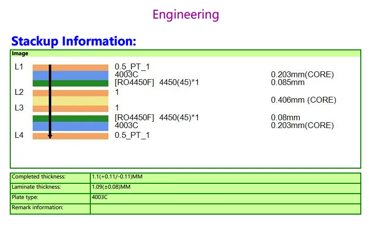
Figure 3: finished board thickness in 1.1mm+/-10%
A further note addresses a stepped region: ENIG is to be applied on the top step surface while the bottom of the step is to expose base material. This instruction is recorded as a fabrication direction rather than as a clearance issue. It does not modify the copper-to-edge or hole-to-edge questions, yet it confirms that the board contains at least one controlled step whose surfaces are treated differently. No interaction between the step and the perimeter clearances is described.
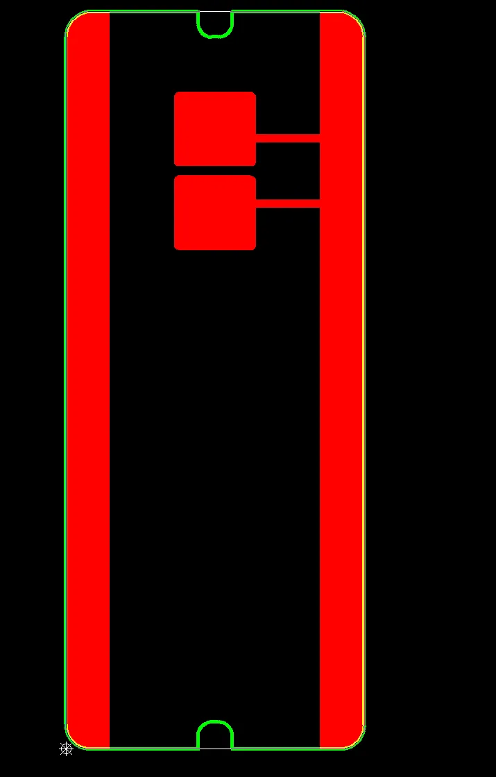
Figure 4: The position indicated, we will fabricate it with top side in ENIG, bottom side with laminate exposoed
PCB Edge Clearance Confirmation and Manufacturing Risks
Both main items are phrased as confirmation requests accompanied by references to figures that are not reproduced in the text record. The factory has identified the copper-to-edge condition as one that will produce exposed copper and the hole-to-edge condition as one that may produce broken holes. No customer reply, no updated Gerber or ODB++ data, and no statement that the clearances have been increased appear in the supplied records. Production confirmation is listed as "No" in the order parameters, consistent with the open engineering questions.
Until confirmation is received, the documented risk remains that the finished edges will expose copper on both inner and outer layers and that perimeter holes may break during or after mechanical forming. The absence of solder mask means any exposed copper will be bare. The ENIG finish will plate only those copper surfaces that remain accessible after etching and before outline routing; copper that is cut by the router will present a raw edge. The records do not indicate whether the customer intends the exposed copper to serve a grounding or shielding function or whether it is unintended. They simply request confirmation of the condition as designed.
CAM Review of Copper-to-Edge and Hole-to-Edge Clearances
The case centers on two clearance observations made during CAM review of a 4-layer Rogers RO4003C board. Copper on the inner and outer layers approaches the outline closely enough that mechanical forming is expected to leave exposed copper at the finished edge. Holes around the perimeter approach the outline closely enough that the finished holes may break. Both observations are submitted for confirmation. Supporting notes address stack-up thickness and a stepped region with selective ENIG, yet neither note supplies additional data that resolves the clearance questions. No design modification, process adjustment, or verification result is recorded. The engineering status is therefore an open request for the customer to accept or revise the copper-to-edge and hole-to-edge geometry before outline fabrication proceeds.