The principal engineering item recorded for this order is the lengthening of the connector fingers by 0.1 mm beyond the original design. The adjustment is made so that the coverlay can press down on the extended copper and thereby help prevent the fingers from peeling. The part is a 4-layer flexible circuit, laser-formed, with overall dimensions of 138.2 × 75 mm. The flexible stack is specified at 0.23 mm ± 0.05 mm; the addition of three discrete 0.075 mm polyimide stiffeners raises the local thickness to 0.31 mm ± 0.05 mm. Copper weight is ½ oz on all layers, the surface finish is ENIG, and both sides are covered with yellow coverlay. Within the same communication the factory also requests confirmation of the stack-up diagram and records that character frames previously placed on pads have been removed from the production file. No reply accepting the finger change, no revised dimensional call-out, and no post-lamination verification appear in the supplied records.
0.1 mm FPC Finger Extension for Coverlay Adhesion
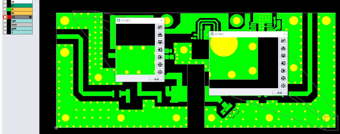
The engineering note states that the fingers are lengthened by 0.1 mm on the original basis for the purpose of allowing the coverlay to press them and prevent peeling. In flexible-circuit practice the coverlay—the polyimide film with its adhesive layer—is laminated over the etched outer copper. At a connector location the coverlay opening must expose the contact area that will receive ENIG while the adhesive edge of the coverlay must still overlap a short length of copper at the root of each finger. That overlapped copper provides the surface to which the adhesive bonds. The 0.1 mm extension supplies precisely this capture length. It is not added to the mating contact zone; it remains under the coverlay after lamination and after the final laser outline is cut.
Without such an overlap the copper finger ends at the edge of the coverlay opening. The free edge then relies solely on the adhesion of the copper to the base film and on any residual adhesive squeeze that may occur during lamination. On a thin flexible construction the peel forces generated by connector insertion, thermal expansion mismatch, or ordinary handling can lift that free edge. Once lifting begins, the finger can delaminate progressively, producing intermittent contact or complete loss of the conductor. The recorded extension places a continuous strip of copper under the coverlay adhesive so that peel and shear loads are transferred into the bonded area rather than concentrated at an unsupported edge.
The note presents the 0.1 mm lengthening as the method applied in the production file. It does not include a measured post-lamination overlap, a peel-strength value, or an explicit statement that the customer has accepted the change. Consequently the figure stands as the documented CAM response to the stated peeling concern rather than as a confirmed final dimension.
4-Layer FPC Stack-Up Thickness and Stiffener Placement
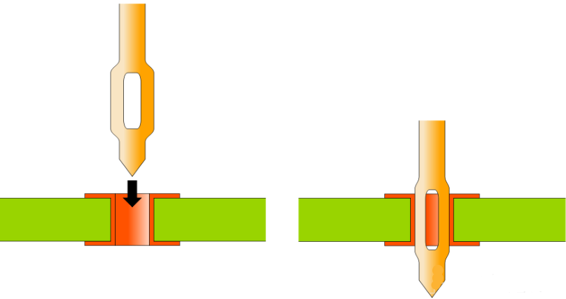
The same communication asks whether the prepared stack-up diagram is acceptable and restates the thickness requirements: 0.23 mm ± 0.05 mm for the flexible circuit ( #FPC-20250917-0076 ) itself and 0.31 mm ± 0.05 mm once the polyimide stiffeners are included. The stiffeners are specified as 0.075 mm thick and three in number. These thickness values establish that the flexible areas are thin and that the stiffeners are localized rather than continuous sheets. Nothing in the records indicates that any stiffener is positioned beneath the finger region. A stiffener under the fingers would increase local rigidity and alter the manner in which the coverlay adhesive loads the copper; the notes contain no such indication. The stack-up confirmation request therefore remains an independent open item that must be resolved before the overall construction, including the finger anchors, can be regarded as approved.

Figure 1: The finger is extended by 0.1 mm from its original length and covered with a film to prevent peeling
Because the flexible PCB thickness is only 0.23 mm, the absolute contribution of the 0.1 mm copper extension is proportionally significant to the local geometry at the coverlay edge. The extension does not change the nominal stack-up thickness calculation, yet it determines whether the adhesive has a defined copper surface to bond to at the transition from covered to exposed copper. The request for stack-up confirmation and the finger-extension note therefore sit side by side: one concerns the global thickness targets, the other concerns the local copper length needed for coverlay retention.

Figure 2: FPC materil thickness is 0.23mm, total thickness including PI stiffener is 0.31mm
FPC CAM File Updates: Removing Silkscreen from Pads
An additional entry in the communication records that character frames drawn on pads were deleted when the production file was prepared. The original artwork is described as red and the production draft as gray. Character frames are legend outlines. Their removal clears printed ink from pad areas that must remain free of contamination for coverlay opening definition and for ENIG plating. The deletion is presented as a completed edit rather than as a proposal still under discussion. While the note does not explicitly connect the legend cleanup to the finger extension, both actions affect the same general regions of the board—areas where coverlay openings, exposed copper, and subsequent surface finish must be clean and accurately defined. The records treat them as concurrent CAM adjustments within one production-file review.

Figure 3: silkscreen printing on pads
FPC Production File Approval and Finger Extension Confirmation
The records end with the statement of the finger lengthening, the stack-up confirmation request, and the legend deletion. No later message indicates that the customer has approved the 0.1 mm extension, that the production files have been updated and re-issued, or that any inspection has verified the presence of copper under the coverlay edge after lamination. In the absence of those follow-up data the engineering status of the change remains that of a documented adjustment whose acceptance and effectiveness have not yet been recorded.
This distinction is material. A proposed or implemented copper-length change of 0.1 mm alters the Gerber or ODB++ data that drives both the imaging of the outer copper and the cutting of the coverlay. Until the change is confirmed, the factory cannot be certain that the final files released to production contain the intended anchor length, nor that the coverlay openings have been sized to leave that length covered. The repeated request to confirm the production draft in the broader communication underscores that the files are still under review.
How FPC Coverlay Anchoring Helps Reduce Copper Finger Peeling
The significance of the case lies in the explicit linkage the records draw between a small dimensional change and a specific mechanical risk. The factory states that the fingers are extended 0.1 mm so the FPC coverlay can press them and prevent peeling. On a ½ oz copper flexible circuit of 0.23 mm thickness the adhesive bond of the coverlay is the primary restraint available at the finger root. By lengthening the copper the production file creates the geometric condition required for that bond to act. The change is local, limited to the connector end, and does not affect the internal layer construction, the impedance status, or the via treatment.
Because no quantitative peel data or post-process measurement is supplied, the records do not demonstrate that the 0.1 mm length is either necessary or sufficient in absolute terms. They demonstrate only that the extension was introduced as the means of providing coverlay capture. For CAM review purposes the actionable content is therefore the presence of the 0.1 mm addition in the production data, the stated purpose of that addition, and the still-open request for stack-up and file confirmation. Resolution of those open items will determine whether the extended fingers proceed into fabrication as documented.
In summary, the engineering communication centers on a single, clearly stated adjustment: the fingers of this 4-layer flexible circuit are lengthened by 0.1 mm so that the coverlay adhesive can press the copper and reduce the risk of peeling. Supporting notes address stack-up thickness confirmation and the removal of pad character frames. No further outcome is recorded. The case remains at the stage of documented CAM intent awaiting confirmation.