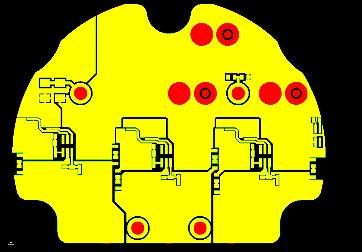
CAM review of blind-via size and edge clearance usually starts with a mismatch in the released package. A named HDI pair may still be drawn at 0.2 mm while the fabricator proposes a smaller laser-drilled finished size. Or a via may sit close enough to the board outline that the released profile could open the barrel. The two questions are different: one concerns the finished via size and forming method; the other concerns the via location relative to the finished profile. Both have to be checked against the released construction and geometry.
On one recent job, in1 (1-2) and in4-back (6-5) measured 0.2 mm. The fabricator stated that HDI blind vias on that construction were laser-drilled, that 0.2 mm was outside the laser-drill range they could support for that job, and proposed 0.1 mm on those two pairs. On another job, vias sat close to the outline, and the note asked whether the released coordinates could result in a broken hole or exposed copper after profiling. Other packages raise the same two questions with different pair names and coordinates.
The three EQs below are examples from those jobs. A missing start layer, stop layer, or HDI drilling note would create a different review. The files being compared remain the same.
| What we saw in the files | Where the files disagree | What the note asked |
|---|---|---|
| in1 (1-2) and in4-back (6-5) blind vias measure 0.2 mm | Named HDI pairs at 0.2 mm against a laser-drill construction on this job | Holes larger than 0.15 mm cannot be laser-made; allow 0.1 mm on those two pairs |
| Via hits sit close to the board outline | Released coordinates against the profile that will cut the board | Confirm whether original data will cause a broken hole and exposed copper |
PCB Blind and Buried Vias in the Released Package
Blind and buried describe which layers the PCB hole starts and stops on. They are not a synonym for a small hole. On the job above, 0.2 mm applied to two named pairs: in1 (1-2) and in4-back (6-5). Those names leave every other via in the ZIP on its own tool. A through via can sit beside them. A buried inner pair can sit beside them on a different span. Plating is a separate flag. Through vias, buried vias, and laser blind vias are often all plated.
Finished size is taken from the hole chart or the drill tool list. Start and stop layers come from that chart when they are written there, or from the stackup and HDI note. The capture pad is the copper on those layers at the same hit. Via-to-edge clearance is the drill coordinate against the board outline. Treating those sources as one tool class detaches the fabricator's question from the hits it actually named.
On the edge note, the word "via" does not identify the layer span. Until the drill is stacked on the pair list and on start/stop copper, those outline hits are drill tools near a profile.
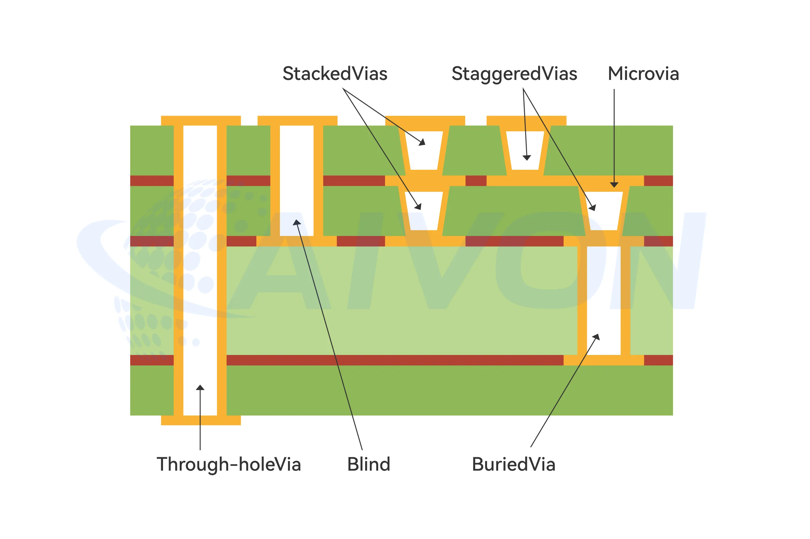
Laser Drilling and Via-to-Edge Clearance on the Blind Via Overlay
Stack the NC drill on 1-2 and 6-5 copper, on the pair list, and on the outline. That stack shows the released diameter, the number of hits, and whether copper on the start and stop layers covers the tool. It also shows how much laminate remains between the drill and the profile, and whether copper at the same coordinate would remain after routing.
Laser drilling is not decided by that overlay alone. On that job it came from the HDI construction together with the fabricator's note that HDI blind vias are laser-made. The overlay also leaves 0.2 mm as a measured size, not a pass/fail result. The 0.15 mm figure was the reason written on that EQ. It is not treated here as a catalog limit for the next board. 0.1 mm is the proposed size. Whether a 0.1 mm tool still sits inside the pad drawn for 0.2 mm, or still serves a via-in-pad land and its net, is checked after that shrink is accepted.
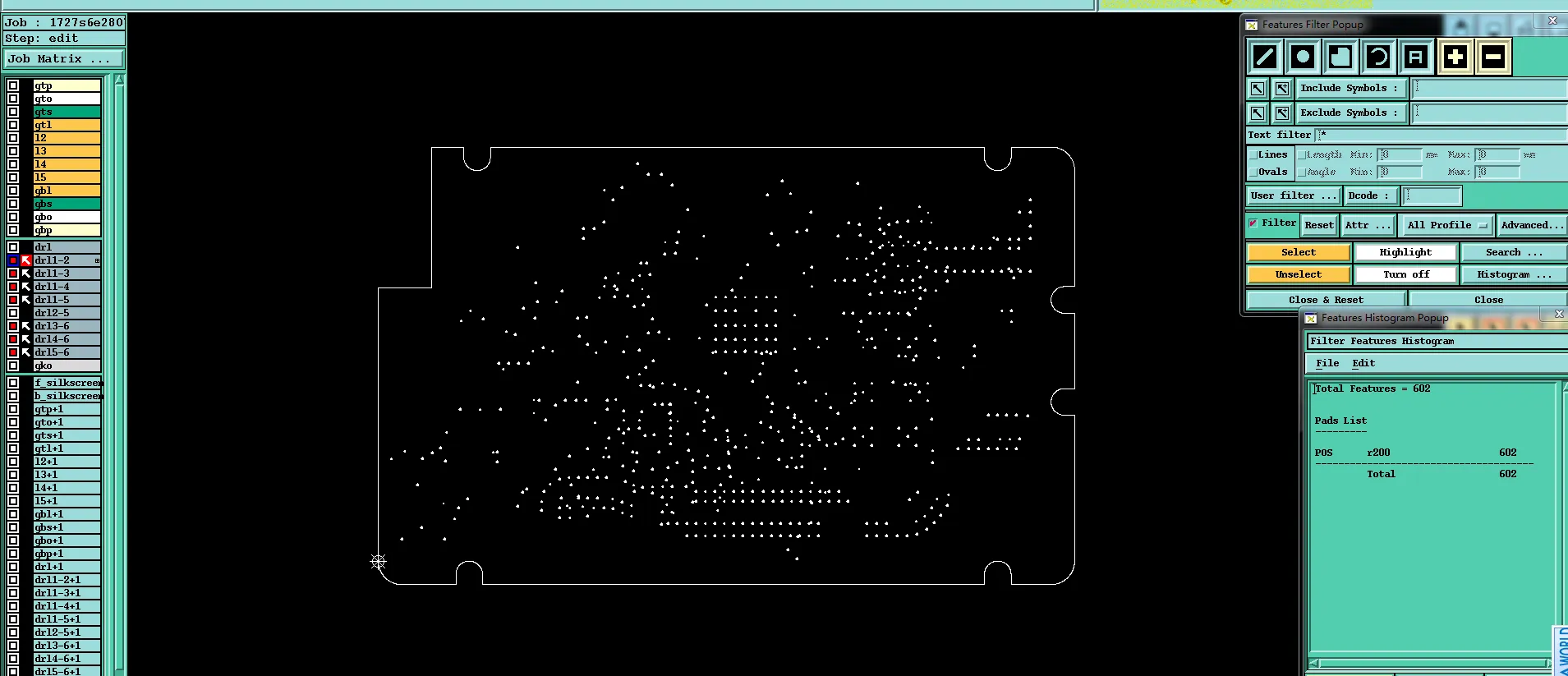
We are drill the blind vias by laser but the min blind hole we can use laser drill is 0.15mm
Toward the outline, the same stack can show a narrow web of laminate. That is the condition behind the broken-hole and exposed-copper wording on the note. It is not, by itself, proof that a finished board will fail. Via-to-edge clearance in this review is drill to outline. Pad-to-edge and pour-to-edge are different edits, unless the via is also the surface land. Microvia, as used here, means the laser 1-N hit on those HDI pairs rather than every small tool on the chart.
| Files stacked | What the overlay shows | What still needs confirmation |
|---|---|---|
| Drill on in1 (1-2) and in4-back (6-5) copper | Released diameter; whether start/stop copper covers the tool | Whether those pairs will be laser-drilled; whether 0.1 mm still fits the pad and the net |
| Hole chart, pair list, stackup or HDI note | Named start and stop layers; whether the construction is called blind, buried, or HDI | A forming method that is not already written; treating 0.15 mm as a drawing number |
| Drill on the board outline | Via-to-edge clearance; copper remaining at that coordinate after the profile is cut | Whether the released coordinates stay, the via or outline moves, or exposure on those hits is accepted |
PCB Laser Drilling When Blind Vias on 1-2 and 6-5 Measure 0.2 mm
Gerber and the tool list on that job showed 0.2 mm on in1 (1-2) and in4-back (6-5). The fabricator grouped three statements with that size: HDI blind vias on this construction are laser-drilled; 0.2 mm is not a conventional laser hole there; a hole larger than 0.15 mm cannot be laser-made. Those statements belong to that package and describe the laser blind via challenges identified on that job. They are not applied here as a default limit on later HDI work.
The proposal was 0.1 mm on those two pairs only. Other vias remain at their released size. The capture pad was drawn around 0.2 mm. If the hits are via-in-pad, or if that diameter was part of a current path or an impedance structure, the land and the net remain the designer's. A smaller tool in the same pad leaves a different annular ring than the one that was released, which is why the shrink waits on a written reply.
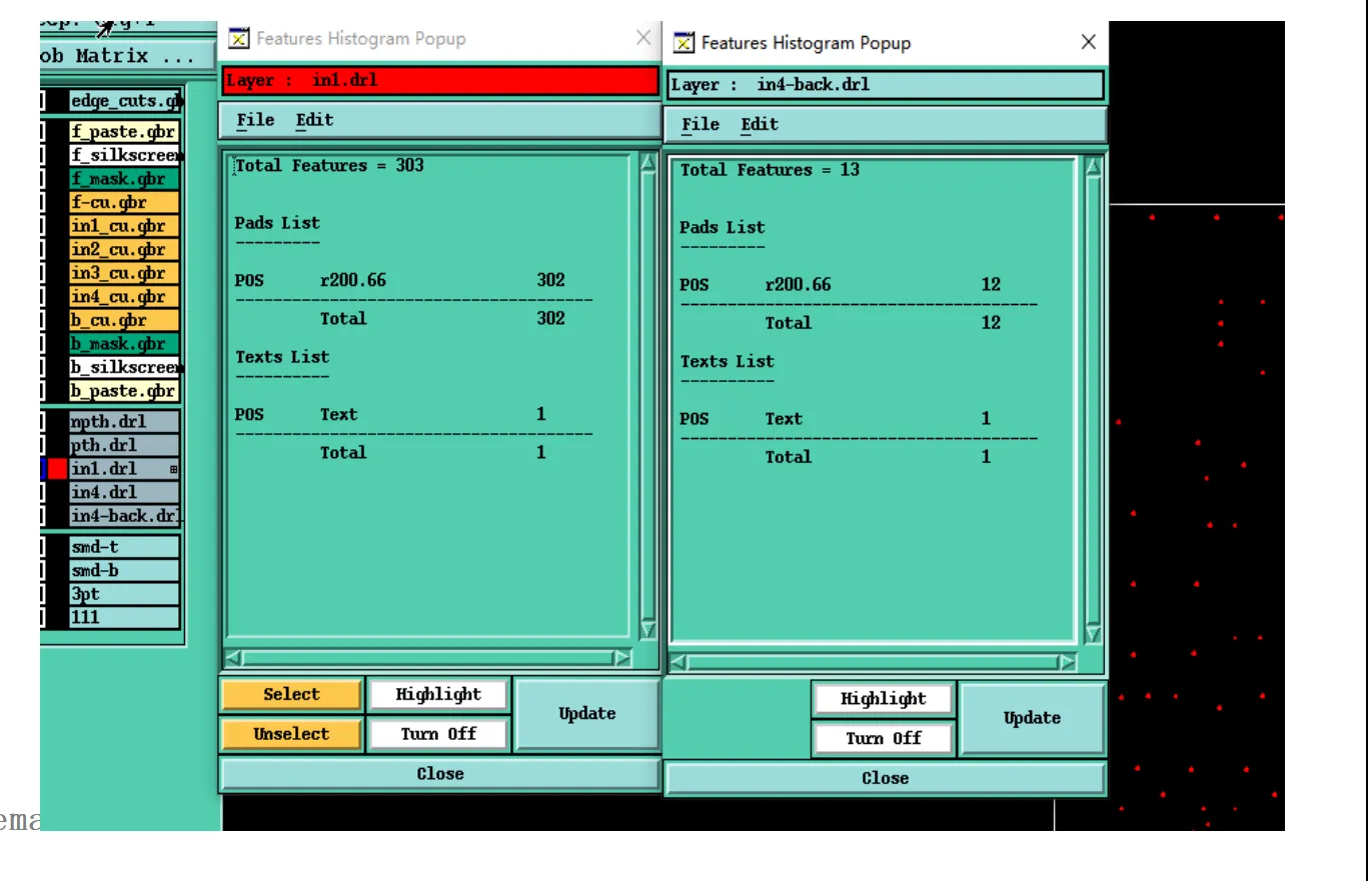
The Gerber files show blind via hole sizes of 0.2mm on in1 (1-2) and in4-back (6-5). This hole size is not a standard laser via diameter.
A mechanically drilled buried via on an inner pair is a different class. The size note did not ask to resize buried vias when the blind pairs changed. Laser drilling in this review is the process attached to 1-2 and 6-5 on that construction.
The close is then one of three written lines. Keep 0.2 mm on those pairs and, if that size is still required, identify another forming method. Accept 0.1 mm on in1 (1-2) and in4-back (6-5) and review the pads against the new diameter. Or return a new diameter with updated pads. Until one of those replies arrives, the released 0.2 mm remains on the named pairs.
PCB Via-to-Edge Clearance When Vias Sit Too Close to the Outline
The measurement is the remaining laminate for the via-to-edge clearance from the via to the profile. On that job, "too close" meant the router or the score would enter the barrel, or the remaining sliver would break and show copper. The package did not include a clearance table that converts the measured web into a pass.
On a plated via, a broken hole is the barrel opening on the finished edge. A pad that also crosses the outline adds surface copper at the same coordinate. That is a different edit from a pour shave and a different edit from an SMT pad trim. Relocating a via and clipping a land are not interchangeable. Forming method matters only as the cut that reaches the via — a routed outline or a V-cut. Remaining thickness after a V-cut, blade angle, and any stamp-hole web on the same tab belong to that other review.
Blind or buried identity does not remove the edge question. A laser microvia on the outline can still open or show copper. Identify the tool, whether it is plated, and the type if the chart gives one. Measure the web. Note outer copper at the same coordinate. The hits then remain, move inboard, are deleted, or the outline moves. Coordinates are not adjusted in CAM without that reply.
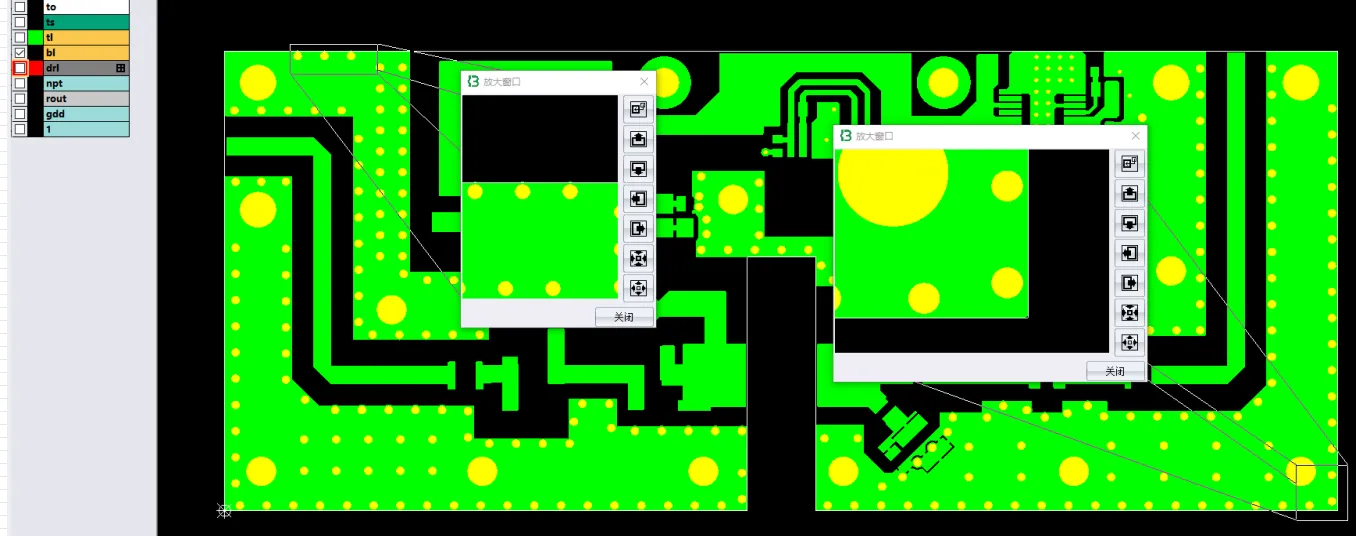
The via holes are too close to the board edge.
Keep the Released Blind Via Size or Confirm Laser Drilling and Via Location
The two findings can close on the same job as two short lines: which pairs at which diameter, and which edge tools at which coordinates or outline. Neither line is an unwritten artwork change.
If the released calls are kept, 0.2 mm remains on 1-2 and 6-5, and the edge vias remain where they were drawn. That close either accepts the process risk named on the note or arrives with a different forming method or a revised outline. CAM does not supply that method on its own.
If 0.1 mm is accepted, it applies to the named laser pairs only. Capture pads and any via-in-pad land are reviewed against the new diameter. Buried vias on other pairs are left at their released size.
If the edge location changes, the via moves inboard, an unused edge via is deleted, or the outline moves. Exposure on those hits is accepted only when that is written. Pulling nearby pour back is not a substitute for moving the via.
| Finding | Keep the release | Accept the factory line | Change the files |
|---|---|---|---|
| 0.2 mm on in1 (1-2) and in4-back (6-5) | Keep 0.2 mm on those pairs; identify another forming method if that size is still required | Allow 0.1 mm on those two pairs only; review capture pads and any via-in-pad land | Customer returns a new diameter and updated pads on the named pairs |
| Via too close to the outline | Keep the released coordinates; customer accepts broken-hole and exposed-copper risk on those hits | Customer accepts exposure on the named tools | Move the via inboard, delete an unused edge via, or move the outline |
The job record keeps the original tool and pair, the measured via-to-edge clearance, the factory proposal, and the customer reply. That record does not treat 0.15 mm as a published laser limit, resize buried vias because the blind pairs changed, or shave a pour in place of moving a via.
PCB Blind Vias, Buried Vias, and Via-to-Edge Clearance Questions From CAM Review
Q1: What is a blind via in a PCB?
A1: A via that starts on one layer and stops before the opposite outer layer. Start and stop come from the hole chart, the pair list, or the stackup, not from hole diameter. in1 (1-2) and in4-back (6-5) on the first job were two named blind pairs. A plated flag by itself does not make the hit blind.
Q2: What is a buried via in a PCB?
A2: A via that starts and stops on inner layers. A mechanically drilled buried via is a different class from a laser blind via that starts on an outer layer. The size note on this job addressed the named 1-2 and 6-5 hits. It did not ask to resize buried vias.
Q3: What is the difference between blind and buried vias?
A3: A blind via reaches one outer layer and stops. A buried via does not reach an outer layer. Both may be plated. Diameter does not identify the type. The pair list does.
Q4: What is a microvia in PCB design?
A4: In this review, the laser 1-N hit on the HDI pairs under discussion. A small through via and a small buried via remain on their own tools until the pair list says otherwise.
Q5: What is laser drilling in PCB manufacturing?
A5: The method the fabricator attached to HDI blind vias on that construction. Overlay of drill to 1-2 and 6-5 copper shows diameter and whether copper covers the tool. Laser as the forming method comes from the construction and the process claim on the note.
Q6: Why are 0.2 mm blind vias a problem for laser drilling?
A6: On that job the fabricator wrote that HDI blind vias are laser-made, that 0.2 mm is not a conventional laser hole on that construction, and that a hole larger than 0.15 mm cannot be laser-made. Those sizes and that reason belong to that EQ. They are not used here as a published maximum laser diameter. The close keeps 0.2 mm, accepts 0.1 mm on those pairs, or returns a new diameter with updated pads.
Q7: If I accept 0.1 mm, do all vias on the board change?
A7: The proposal named in1 (1-2) and in4-back (6-5) only. Other tools remain at their released size. Pads on those two pairs still need to be reviewed against the new diameter.
Q8: What is via-to-edge clearance on a PCB?
A8: The distance from the via drill to the board outline. It is a different measurement from pad-to-edge clearance or copper-to-edge clearance on a pour. Those are separate edits unless the via is also the surface land.
Q9: How close can a via be to the board edge?
A9: This review does not publish a minimum. On the job that raised the question, the fabricator named broken hole and exposed copper if the original coordinates were formed as drawn. Overlay shows the remaining web. The close keeps those coordinates, moves the via or the outline, or accepts exposure on those hits.