Introduction
This 6-layer HDI board was a typical high-density consumer electronics application with 0.2mm laser blind vias, 1.0mm finished thickness, and ENIG surface finish. While the design looked straightforward on paper, the CAM engineering review revealed multiple manufacturability conflicts that required immediate clarification.
HDI boards with mixed blind/buried vias and tight SMD geometries frequently trigger engineering questions (EQs) because the gap between design intent and actual production capability can be significant. Our CAM team spent considerable time analyzing the Gerber data, stackup, and panelization before we could safely release the job for production.
In this real engineering case, I will walk through the major issues we discovered, the risks they posed, and how we resolved them. These are the exact kinds of problems that cause delays, yield loss, or field failures if not caught early.
6-Layer Thin HDI PCB Order Specifications and Stackup Details
This was a 6-layer HDI board (#HDI-20260418-083) (2 steps) with 1.0mm finished thickness. Outer copper was specified as 0.5oz base + 1oz plated, inner layers standard 1oz. Minimum hole size included 0.2mm laser blind vias. The board used ENIG surface finish, 100% flying probe test, and mechanical routing with stamp hole depanelization.
Customer requested 15 pieces (5 sets) with original panelization of 3x1. The design included buried vias on inner layers and blind vias from L1-2 and L5-6. Impedance control was required on L1. The stackup was customer-specified with Shengyi S1000H material, but our factory standard TG150 cores and prepregs needed alignment.
Critical DFM Issues Identified in CAM Review for Thin HDI PCB
1. HDI PCB Printing Challenges: Solder Mask Bridge Failures and Silkscreen Overlap on Tight SMD Pads
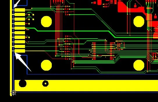
The most immediate and visible problem was in the SMD pad layout. Multiple areas showed pad-to-pad spacing too narrow to reliably form a solder mask bridge. Our standard process requires at least 19mil effective spacing (including character line width 6mil + 6mil×2 clearance + compensation) to guarantee a stable solder mask dam.H6P-C7R-AI19146A
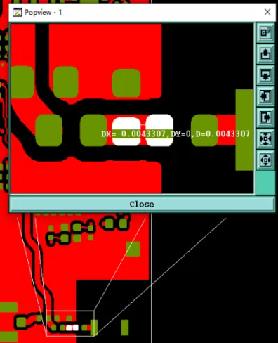
Figure 1: Pad-to-pad spacing is too narrow to reliably form a solder mask bridge.
We noticed several silkscreen characters placed directly on or overlapping solder mask openings. Our engineer flagged this immediately: “If printed on exposed copper, the legend ink will have poor adhesion and is likely to peel during assembly or in the field, affecting both appearance and long-term reliability.”
Figure 2: Silkscreen characters placed directly on or overlapping solder mask openings
If ignored, this would result in missing solder mask bridges, solder bridging during SMT, or legend ink flaking that contaminates pads. We requested customer confirmation and prepared adjusted solder mask files with bridged openings where possible.
| Parameter | Standard Requirement | Consequence of Violation |
|---|---|---|
| Pad-to-Pad Spacing | ≥19mil effective (incl. compensation) | Missing bridges, solder shorts in SMT |
| Silkscreen Placement | Avoid overlap with openings | Poor adhesion, ink flaking, contamination |
Table 1: Solder Mask Bridge Requirements for Tight SMD Pads
2. Low Inner Layer Copper Density and Resin Starvation Risk During Lamination
Layer L4 (in3) showed only routing traces and isolated pads with almost no copper pour. This extremely low copper density creates serious pressure imbalance during lamination.
Figure 3: Low copper density on inner layers
Our CAM engineer identified this right away: “With such low resin-to-copper ratio, we risk resin starvation, voids, or even delamination under thermal stress.” According to typical IPC-6012 Class 2 considerations, unbalanced copper distribution significantly increases the chance of board warpage and interlayer separation, especially in a 1.0mm thin HDI construction.
Figure 4: Copper-poured diagram
Had production continued without adjustment, the board could suffer from “measling,” resin voids, or complete delamination after reflow, leading to scrap or latent field failures.
Low copper density on inner layers like L4 increases resin flow imbalance risks.
| Layer Characteristic | Typical Recommendation | Risk if Not Balanced |
|---|---|---|
| Inner Layer Copper Density (e.g., L4) | Adequate copper pour for pressure balance | Resin starvation, voids, warpage, delamination |
| Overall Board Thickness | 1.0mm HDI construction | Amplified thermal stress issues |
Table 2: Copper Density Comparison and Lamination Risks in Thin HDI Boards
3. 0.2mm Laser Blind Vias and Buried Via Plugging Reliability in HDI Boards
The Gerber specified 0.2mm blind vias for laser drilling on L1-2 and L5-6. While 0.2mm is within our laser capability, it is not our most common production size, requiring process confirmation for aspect ratio and plating reliability.
Figure 5: Specified 0.2mm blind vias for laser drilling on L1-2 and L5-6
Additionally, the 0.6mm buried vias on inner layers were too large for reliable via plugging (hole fill). Large plugged holes at this diameter increase the risk of voids or incomplete fill, which can cause reliability issues in HDI structures.

Figure 6: The 0.6mm buried vias
We confirmed the via types and suggested minor adjustments to via attributes to ensure consistent plating and filling.
4. Panelization Redesign for Better Material Utilization in Thin HDI Production
Customer requested 3x1 panelization, but this created excessive waste on the process edges. Our team redesigned to 3x2 (102×93mm) with stamp hole depanelization. This change improved material utilization and reduced waste without affecting the final board size.
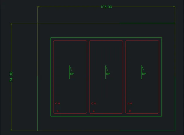
Figure 7: Requested 3x1 panelization
We also addressed the material specification. Customer called for Shengyi S1000H TG150, but our factory standard equivalent TG150 material was readily available. Using the specified material would have extended lead time significantly. After confirmation, we used our matched factory material.
5. Impedance Control & Stackup Confirmation
The original Gerber trace widths did not meet the target impedance with our production stackup. L1 had a confirmed 50Ω requirement. Our engineering team adjusted trace widths and confirmed the full stackup details with the customer to ensure impedance compliance after plating.This adjustment was necessary because the final copper thickness after plating, combined with the specific dielectric materials and thicknesses in the stackup, directly affects impedance values. We provided the customer with calculated trace width recommendations based on our validated stackup model.
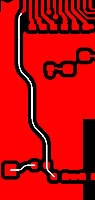
Figure 8: Confirmed 50Ω requirement
Proper stackup confirmation early in the process helps prevent costly revisions later and ensures signal integrity meets the design requirements across the 6-layer HDI PCB construction.
Key Manufacturing Risks and DFM Lessons from This Thin HDI PCB Case
This case highlights several recurring DFM pain points in HDI designs:
- Tight SMD geometries that violate solder mask bridge rules are among the most common triggers for EQs and SMT defects.
- Isolated routing layers without copper balancing frequently cause lamination problems in thin boards.
- Via sizing must match the factory’s laser and plating process capabilities — “standard” customer via sizes are not always optimal.
- Panelization decisions should consider material utilization early in the design phase.
Ignoring these would have led to solder shorts, delamination, poor via reliability, excessive material cost, and potential delivery delays.
CAM Engineering Resolutions and Customer Approval Process
Our CAM engineers prepared a complete set of adjusted production files: updated solder mask with feasible bridges, copper balancing where possible, revised panelization, and confirmed stackup with impedance adjustments. All changes were clearly documented and sent back to the customer for approval.
After receiving confirmation on material, silkscreen removal on BOT layer, and impedance targets, the job was released for production with optimized parameters. The first-article panels passed our internal quality checks before full run.
Successful Production Outcome After EQ Resolutions
All engineering questions were resolved through clear communication. Production files were updated, panelization optimized, and the boards successfully moved into fabrication. The 15 pieces were completed within the agreed 21-day lead time.
Essential DFM Tips for Thin HDI PCB Designers to Avoid Common EQs
- Always verify minimum solder mask bridge requirements (typically ≥0.15–0.20mm depending on process) against your SMD pad spacing.
- Avoid placing silkscreen legend on exposed copper pads or openings.
- Include adequate copper pour on all layers for balanced lamination, especially in HDI and thin boards.
- Coordinate via sizes (blind, buried) with your manufacturer’s standard laser and plating capabilities.
- Provide clear impedance requirements and reference layers early.
- Consider panelization and material utilization during the layout phase to reduce cost and waste.
- Use consistent layer naming and include fabrication notes in the Gerber/ODB package.
FAQ
Q1: Why can't PCB factories reliably produce solder mask bridges on very tight SMD pads?
A1: Solder mask application has physical limits on dam width and registration tolerance. Below ~19mil effective spacing (including compensation), the bridge becomes too thin, prone to breaking or incomplete coverage, leading to solder shorts during assembly.
Q2: What happens if inner layers have very low copper density?
A2: During lamination, resin flows unevenly, causing resin starvation, voids, or board warpage. In severe cases, this leads to delamination under thermal cycling or assembly reflow.
Q3: What are common HDI PCB printing challenges with solder mask and silkscreen?
A3: In high-density designs, tight SMD pad spacing often prevents reliable solder mask bridges, while silkscreen placed on exposed copper leads to adhesion failures. Factories recommend maintaining minimum dam widths and keeping legend off pads to prevent SMT defects and long-term reliability issues. Early CAM review catches these before production.
Q4: Is 0.2mm a standard laser blind via size?
A4: It is manufacturable but not the most common. Factories prefer sizes that balance aspect ratio, plating reliability, and laser process window. Confirmation is always needed for non-standard vias.
Q5: Why must silkscreen be kept off exposed copper pads?
A5: Legend ink does not adhere well to bare copper or ENIG surface. It flakes easily during handling, assembly, or use, creating cosmetic defects and potential contamination.
Q6: How important is copper balancing in HDI boards?
A6: Critical. Unbalanced copper distribution is one of the leading causes of warpage and delamination in multilayer and HDI constructions, especially at 1.0mm or thinner.