










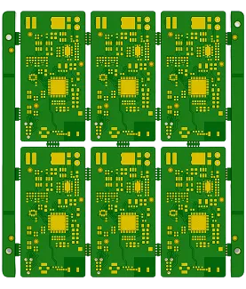
PCB Specifications
| Parameter | Value | Parameter | Value |
|---|---|---|---|
| PCB Type | HDI PCB | Quantity | 15 pcs |
| Layers | 6 Layers | Board Type | Panel PCB |
| Dimensions | 25 x 50 mm | Copper Weight | 1oz |
| Thickness | 1 mm | Min Track / Spacing | 6/6mil↑ |
| Surface Finish | ENIG (Immersion Gold) | Min Hole Size | 0.2mm |
| Solder Mask | Green | Silkscreen | White |
| HDI Structure | 2 | Blind/Buried Vias | Yes |
Manufacturing Timeline
Logistics Information
Key Manufacturing Processes
Manufacturing Summary
This 6-layer HDI PCB was manufactured on FR-4 TG150 material with a finished thickness of 1.0 mm and board size of 25 × 50 mm. The build used 0.5 oz outer copper and 1 oz inner layers, 0.2 mm minimum holes, 6 mil line/space, and ENIG finish. Fifteen pieces were produced in 3×1 panel format with laser-drilled blind vias (2-step HDI) and delivered after 100% flying probe testing within the 21-day lead time. The small form factor combined with blind via requirements and controlled impedance on L1 demanded precise stackup design and process parameter control.
Multiple DFM issues were resolved during EQ review. Gerber data showed insufficient solder mask bridge width between SMD pads, character placement on openings risking ink adhesion failure, and low copper density on inner layers that could cause resin starvation during lamination. Blind via diameters were confirmed for laser drilling capability, while panelization was optimized from the original layout to a 3×2 arrangement (102 × 93 mm with stamp holes) to reduce material waste and improve handling. Stackup was adjusted using standard in-house TG150 cores and prepregs after material availability confirmation. These solder mask bridge and resin density adjustments were implemented to ensure reliable via formation and surface quality.
All fifteen boards passed electrical testing, visual inspection, and final quality checks with stable impedance and clean via structures. The order was shipped with electrical test reports and certificate of conformity, demonstrating consistent results on this compact 6-layer HDI configuration.
Explore More PCB Manufacturing Resources
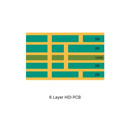
6 Layer HDI PCB Manufacturing Insights
This page details production methods, specification ranges, and optimization techniques for reliable 6 layer HDI circuit boards.
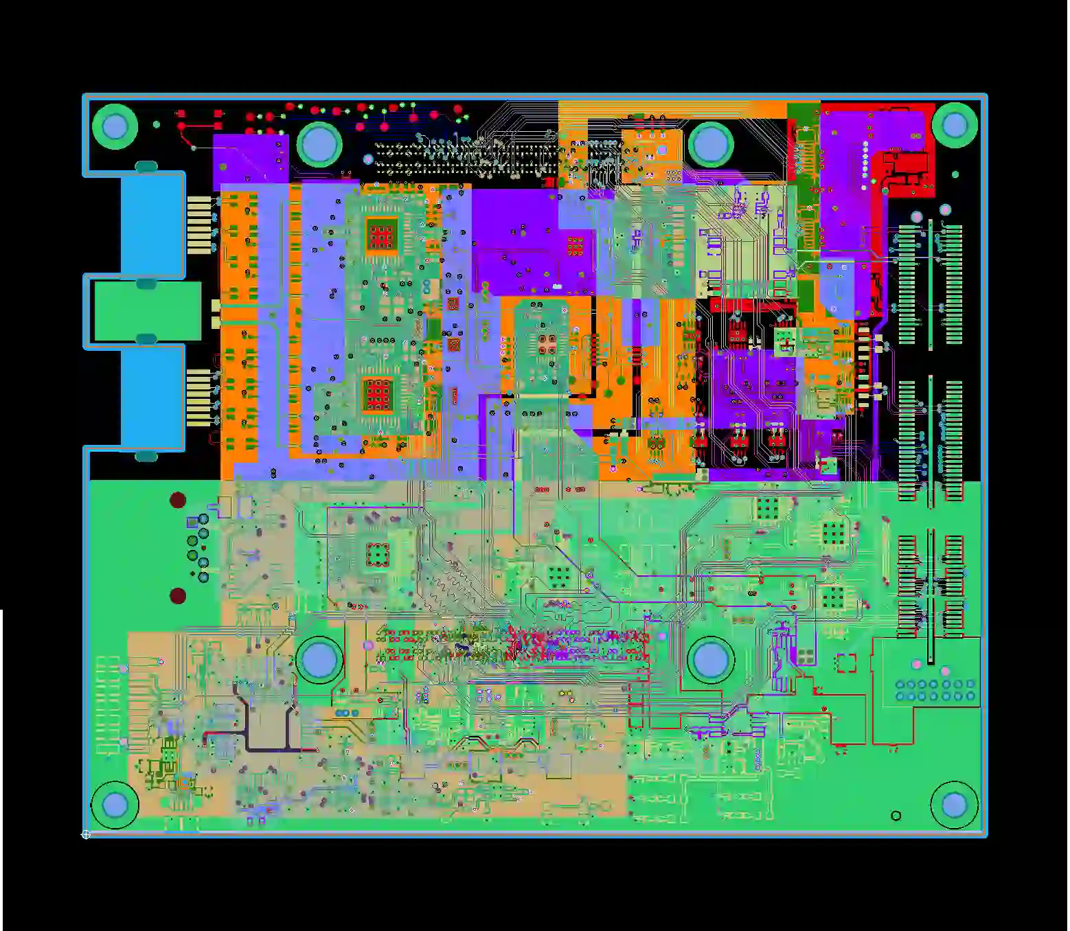
Multilayer HDI PCB Common Engineering Queries in Manufacturing
Senior PCB manufacturing engineer shares real factory insights on common engineering queries for multilayer HDI PCBs including 4 Layer HDI PCB, 6 Layer HDI PCB, 8 Layer HDI PCB, and 10 Layer HDI PCB. Learn about microvia stacking, registration challenges, impedance control, and practical DFM tips to reduce EQs and improve production yield.
Real Production Records
| Order ID | PCB Type | Layers | Dimensions | Solder Mask | Surface Finish | Quantity | Action |
|---|---|---|---|---|---|---|---|
| HDI-20260729-036 | HDI PCB | 8 | 97 x 93.4 | Black | ENIG (Immersion Gold) | 100 | View detail |
| HDI-20260720-0001 | HDI PCB | 8 | 188 x 100 | Matte Black | ENIG (Immersion Gold) | 125 | View detail |
| HDI-20260718-0002 | HDI PCB | 4 | 37 x 26.6 | Green | ENIG (Immersion Gold) | 20 | View detail |


