Introduction
This 6-layer 2nd order HDI board measures only 44 × 28 mm with a finished thickness of 1.0 mm and requires controlled impedance. The design incorporates blind vias and calls for resin plugging on through holes. Small form-factor HDI boards with mixed via structures frequently trigger detailed CAM review because laser drilling limits, lamination sequence, and solder mask definition interact directly with the final stackup. Before any production files are released, our engineering team performs a full DFM check to catch conflicts between customer intent and actual manufacturing capability. In this order the review surfaced six distinct engineering questions that required clarification before the job could move forward.
6-Layer 1.0mm 2nd Order HDI PCB Order Specifications
The board is fabricated on Shengyi S1000H FR-4 with a Tg of 150 °C (#FR4-20260312-006). Both inner and outer copper are specified at 1 oz. Minimum hole size is 0.20 mm and the design calls for 3 mil line/space. Surface finish is ENIG with 1 µ" gold. Solder mask is blue on both sides and legend is white. The order requests 5 sets, 100 % flying-probe test, and impedance control, although no impedance report was supplied with the original data package. Panelization is listed as 1 × 1 with 9 mm process edges and 2.00 × 2.00 mm routing slots. The customer indicated blind/buried vias are present and explicitly requested resin plugging for through holes, while the initial fabrication notes showed only via tenting (cover oil). The stackup was later revised by the customer to support 2nd-order HDI construction.
Engineering Questions Identified in HDI PCB CAM Review
Production Number Placement and Panelization Configuration Mismatch
The customer asked how the factory production number would be added to the board. Our CAM team confirmed the standard location on the copper side within the process edge area to avoid any impact on the functional circuitry or solder mask.
The original order listed 1 × 1 panelization, yet the customer had specified 1 × 2. We provided an optimized 1 × 1 layout using straight panelization with bridge connections and stamp holes. The customer reviewed the revised panel drawing and confirmed acceptance. This change reduced material waste while maintaining the required process edges and routing slots.
![]()
Figure 1: Required panel separating way by the customer
Inner Copper Confirmation and Revised HDI Stackup for Impedance
The customer requested confirmation of inner layer copper thickness. We verified that the 1 oz copper specified on the order matches the standard base foil used for this stackup. No adjustment was required.
![]()
Figure 2: Inner layer copper thickness: 1 oz Cu
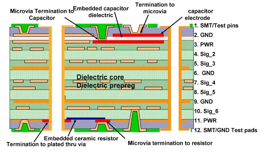
The factory initially prepared a conventional press cycle, but the board is a 2nd order HDI construction. The customer supplied a revised lamination sequence and impedance targets. Our engineering team reviewed the new stackup drawing and confirmed that the layer sequence, dielectric thicknesses, and copper weights support the required impedance values. After cross-checking the blind via locations against the new build-up, we approved the optimized stackup. We noticed that the revised sequence also improves resin flow around the buried vias, reducing the chance of voids during lamination.
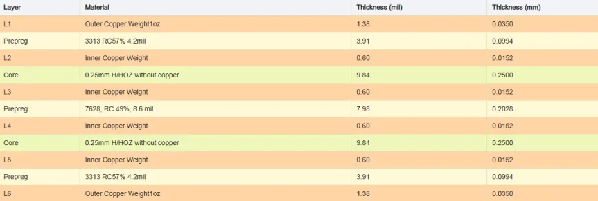
Figure 3: Standard/Finished thickness
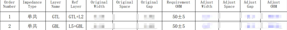
Figure 4: Impedance Info
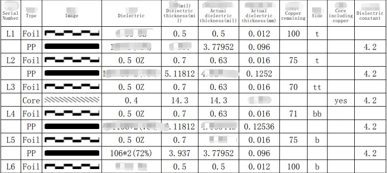
Figure 5: Stackup diagram
Blind Via Diameter and Laser Drilling Limit
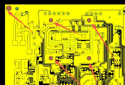
Several blind vias exceeded 0.15 mm in diameter. Our CAM engineer identified that laser drilling on this equipment is limited to 0.15 mm maximum for reliable via formation. We asked the customer to confirm whether these larger blind vias could be reduced or converted to mechanical drilling where possible. If the oversized blind vias had proceeded unchanged, drill breakout or incomplete plating could have occurred, leading to open circuits or unreliable interlayer connections in the HDI build-up.

Figure 6: Blind vias exceeded 0.15 mm in diameter.
Potential consequence if ignored: Oversized blind vias drilled mechanically instead of laser would risk pad breakout and plating voids, resulting in intermittent opens after thermal cycling and low first-pass yield.
Through-Hole Via Plugging Process
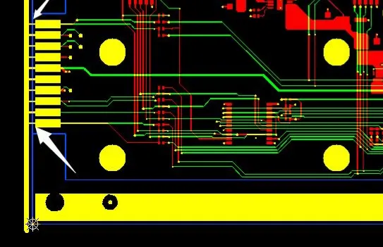
The customer explicitly required resin plugging on through holes, yet the initial fabrication notes indicated only via tenting (cover oil). Our engineer confirmed the resin plugging requirement and updated the production data accordingly. We noticed that without resin fill, the vias could trap air or plating solution during ENIG processing, creating voids that later cause via cracking or outgassing during assembly reflow.

Figure 7: Fabrication notes for tenting vias
Potential consequence if ignored: Unfilled vias in a 1.0 mm thick HDI board would increase the risk of plating solution entrapment, leading to corrosion or delamination around the via barrel after multiple thermal excursions.
Narrow Solder Mask Bridge Spacing on Fine-Pitch Pads
Several pad pairs showed a solder mask opening spacing of less than 6 mil. Our CAM team flagged that a reliable solder mask bridge cannot be formed at this distance on blue LPI material. We requested customer confirmation on whether the pads could be adjusted or if the bridge requirement could be relaxed. According to typical IPC-A-600 considerations for solder mask definition, such narrow bridges frequently result in mask lifting or bridging during development, exposing adjacent copper and creating potential short circuits during assembly.
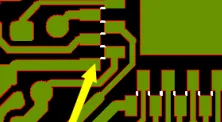
Figure 8: Less than 6 mil solder mask opening spacing of pad pairs
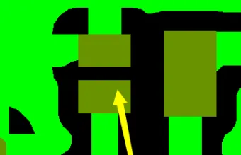
Figure 9: Revised pad for reliable solder mask bridge
Potential consequence if ignored: Solder mask bridge failure would allow solder to bridge between pads during reflow, causing electrical shorts on the assembled board and requiring costly rework or scrap.
DFM Risks in Small Form-Factor 2nd Order HDI PCBs
This case highlights several recurring DFM pitfalls on small 2nd-order HDI designs. Blind via diameter limits are frequently overlooked when designers copy via sizes from previous non-HDI boards. Resin plugging is often specified late in the order without updating the via attribute in the Gerber or ODB++ data. Narrow solder mask bridges remain one of the most common sources of assembly defects on fine-pitch layouts. When stackup changes are submitted after the initial review, impedance targets must be re-validated against the new dielectric thicknesses; otherwise signal integrity issues appear only after boards are assembled. Each of these issues, if left unresolved, extends engineering communication cycles and risks production delays or yield loss.
| Issue | Risk if Unresolved | Resolution |
|---|---|---|
| Blind Via Diameter | Breakout or plating voids | Reduced size or mechanical drill conversion |
| Resin Filled Via | Voids, entrapment, cracking | Updated attributes and notes |
| Solder Mask Bridge | Mask lifting or shorts | Pad adjustment to ≥6 mil web |
| HDI Stackup Revision | Impedance mismatch | Re-validated with new build-up |
Table 1: Key DFM Risks in This 6-Layer HDI PCB
Resolution of Via, Stackup, and Mask EQs in HDI Design
Our CAM engineer updated the via attributes to resin plugging and adjusted the production notes accordingly. The panel was locked at the optimized 1 × 1 configuration with customer sign-off. The revised HDI stackup and impedance targets were accepted after our review confirmed compatibility with the blind via locations. For the oversized blind vias, the customer agreed to reduce several diameters to 0.15 mm or below; the remaining larger vias were converted to mechanical drill where the design allowed. The solder mask bridge locations were reviewed and the customer accepted a minor pad adjustment on the most critical pairs to achieve a minimum 6 mil mask web. After all clarifications were incorporated, the files were re-generated and released for production.
Successful Production After HDI DFM Adjustments
All engineering questions received customer confirmation. The stackup, via plugging process, panel layout, and solder mask parameters were aligned with manufacturing capability. CAM review was completed and the job was approved for release to the production floor with the updated 2nd-order HDI build-up and resin-filled through holes.
DFM Best Practices for Resin Filled Via HDI PCBs
- Always specify via plugging requirements (resin vs. tenting) explicitly in both the fabrication notes and via attributes.
- Verify blind via diameters against the supplier's laser drilling limit (typically ≤ 0.15 mm) before finalizing the layout.
- Maintain a minimum 6 mil solder mask web between pads on LPI processes; adjust pad spacing early if needed.
- When revising the stackup for HDI, re-run impedance calculations and provide the updated targets with the new build-up drawing.
- Confirm panelization requirements (1 × 1 vs. 1 × 2) in the initial order to avoid mid-review changes.
- Include clear layer naming and via type definitions in the Gerber or ODB++ package to reduce interpretation errors.
- Document any special process needs (resin plug, specific gold thickness, etc.) in a separate fabrication note file rather than relying solely on the board outline layer.
FAQ
Q1: Why do PCB factories require confirmation on resin plugging for through holes?
A1: Resin plugging prevents air entrapment and plating solution residue inside vias. Without it, voids can form during lamination or ENIG processing, leading to via cracking or corrosion after assembly thermal cycles.
Q2: What happens if blind vias exceed the laser drilling limit?
A2: Vias larger than the equipment limit must be drilled mechanically, which increases the risk of pad breakout, plating voids, and unreliable interlayer connections in HDI constructions.
Q3: Why can't a solder mask bridge be formed when spacing is below 6 mil?
A3: LPI solder mask requires sufficient web width for proper adhesion and development. Narrow bridges often lift or bridge during processing, exposing copper and creating assembly short risks.
Q4: How does a revised HDI stackup affect impedance control?
A4: Changing dielectric thicknesses or copper weights alters the impedance of controlled traces. The stackup must be re-validated against the target values before production to avoid signal integrity issues.
Q5: Why is panelization sometimes changed during engineering review?
A5: Factories optimize panel layout for material utilization and process edge requirements. Early confirmation prevents later conflicts with routing slots or depanelization methods.