In HDI production we handle the solder mask process by running tight exposure parameters combined with targeted window compensation and minimum bridge width rules that match our actual lamination and development capabilities. CAM engineers review every HDI job for solder mask to panel registration tolerance, adjust the openings by 0.015–0.025 mm depending on copper height and material, and set bridge widths no smaller than 0.08 mm for standard fine pitch before releasing to production.
How registration drives the need for solder mask compensation in HDI panels
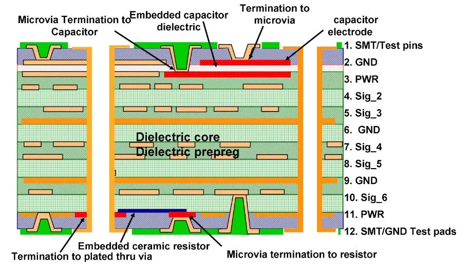
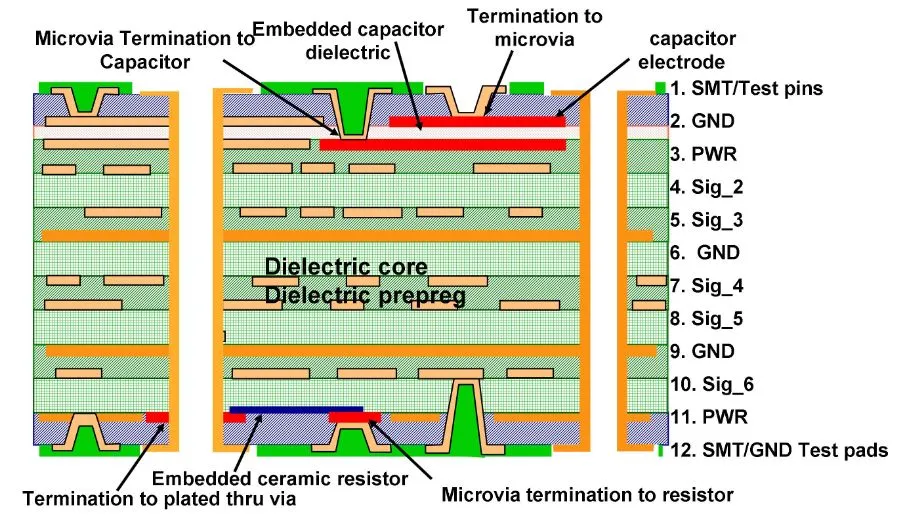
What we typically see on the CAM side during HDI solder mask process review is that multilayer registration from sequential lamination already consumes part of the available tolerance budget. Each lamination cycle introduces slight movement, especially around dense microvia fields. By the time we reach solder mask application the panel has accumulated 0.05–0.075 mm total variation across the working area. This forces us to compensate mask openings outward so that pads remain fully exposed even when the mask shifts within our process capability.
On high layer count HDI boards the copper surface also varies in height due to plating distribution. Thicker copper in dense areas makes the mask sit higher, changing the effective exposure energy needed at those locations. Without compensation the developed openings either undersize or bridge between adjacent pads.
Why solder mask exposure becomes more sensitive in HDI production
HDI designs push finer features and tighter pitch, which directly hits our exposure equipment limits. Standard exposure uses 5–7 mil lines but HDI frequently requires 3–4 mil solder mask dams. The photoimageable mask thickness we apply (typically 18–25 µm after cure) combined with the uneven topography from filled or capped microvias creates focus challenges. Exposure energy that works for flat areas overexposes in recessed zones or leaves residue in high copper areas.
Panel size also matters. Larger 24 × 28 inch panels used for volume HDI production magnify any thermal expansion during drying and exposure, making uniform mask definition harder to maintain across the entire sheet.
What happens when window compensation and bridge width are not properly controlled
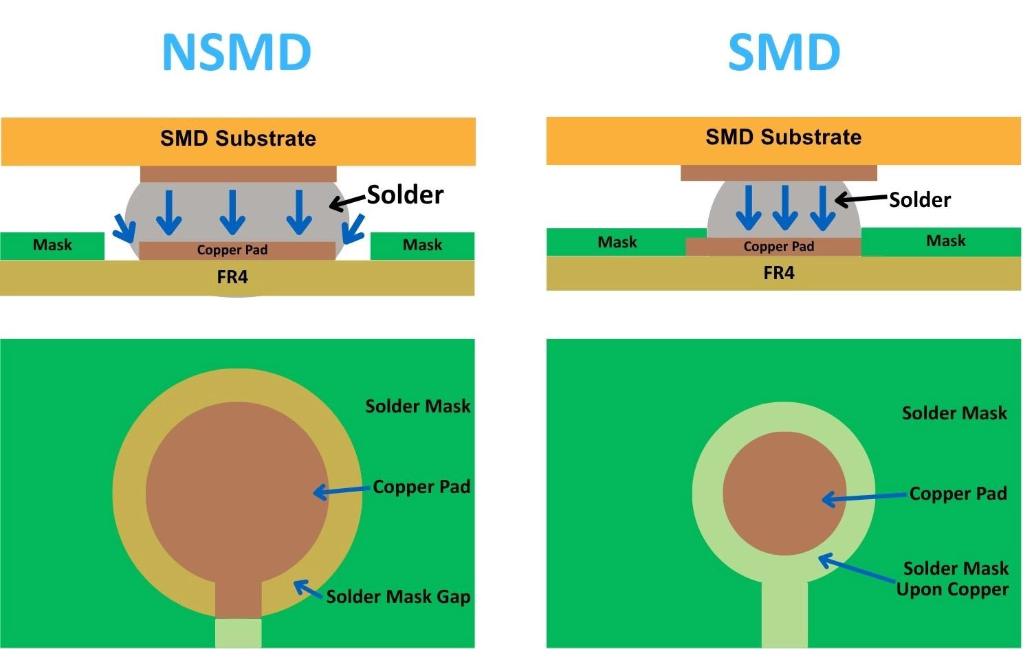
If we skip compensation or run with insufficient bridge width the most common result is partial pad coverage after development. This leads to poor solderability, open joints during assembly, or solder mask residue causing non-wetting. In tighter cases the mask bridges between pads shrink below 0.05 mm and break during chemical processing or handling, creating shorts that only appear after assembly.
Yield drops quickly. We have seen batches where uncompensated HDI solder mask process dropped first-pass yield from 96 % to under 70 % because of mask misalignment on outer layers. Rework becomes expensive since HDI boards often carry high value from buried vias and sequential builds. Worst case we scrap the panel when the shift affects multiple inner layers that cannot be reworked.
Typical defects observed in production
- Solder mask encroachment on fine pitch pads reducing effective land area
- Broken mask dams between 0.4 mm pitch components
- Residue in microvia entrances affecting reliability
- Registration shift causing exposed copper on traces near pads
How factories adjust exposure parameters for reliable HDI solder mask process
We start by measuring actual panel registration from the drill or routing data. Our standard practice for HDI is to apply a 0.02 mm uniform expansion to all solder mask openings unless the design has special requirements. For high density BGA areas we calculate compensation individually based on local copper density and via fill height.
Exposure is done on high-resolution LED or laser direct imaging systems calibrated daily. We run step wedges on every job to verify energy settings. Typical exposure time gets adjusted 5–10 % higher for HDI panels to ensure full polymerization in thicker mask areas while avoiding overexposure that narrows the dams. Development parameters stay aggressive enough to clear small windows but controlled to protect the 0.08 mm minimum bridge we set in CAM.
Bridge width control and its impact on HDI yield
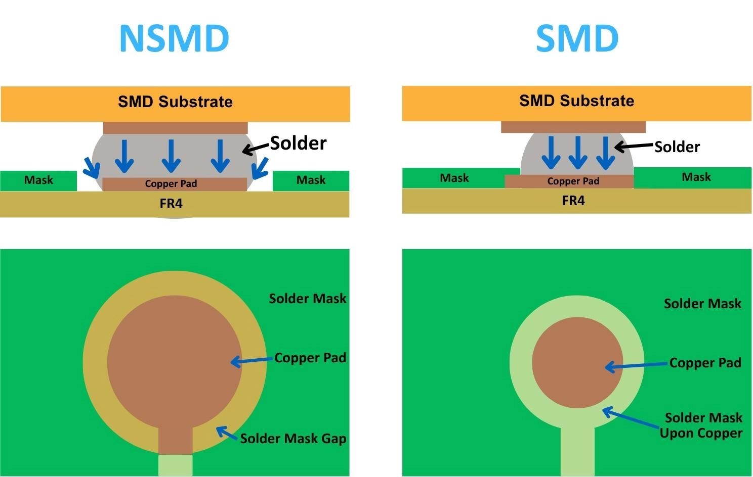
Bridge width is the single most important number we watch in the HDI solder mask process. Our factory rule for standard production is 0.08 mm minimum after compensation. For 0.35 mm pitch or below we may request the designer to increase pad spacing or accept lower yield expectations. During CAM we run design rule checks that simulate worst-case registration and only approve files where the remaining mask dam stays above 0.06 mm even at tolerance extremes.
When copper distribution is uneven we sometimes add local copper balancing or adjust plating parameters upstream, but the mask compensation remains the final safeguard. Pre-bake and post-exposure bake temperatures are tightly controlled to minimize shrinkage that could narrow the bridges further.
Practical solutions factories use during production runs
Most factories solve HDI solder mask challenges by combining several adjustments. We apply scaling factors derived from historical panel movement data rather than theoretical values. For each job the CAM operator checks the solder mask against the outer layer drill program and applies offset if needed. Automated optical inspection after development catches any remaining issues early.
In high volume we run test coupons with the same compensation on every panel and measure opening sizes with AOI. If the data drifts we tweak exposure energy or mask viscosity before the next lot. This data-driven approach keeps the overall HDI solder mask process yield above 92 % even on complex designs.
When we can relax the compensation rules
Exceptions are allowed on simpler HDI boards with larger pitch components and good copper balance. If the design uses 0.5 mm BGA or above and has fewer than four sequential laminations we may reduce compensation to 0.01 mm and allow 0.07 mm bridges. Prototype runs sometimes accept higher risk for speed, but production orders stay under strict control. The trade-off is always between yield and design density — pushing too far simply increases cost through lower yields and longer lead times.
Communicating early during DFM review gives us the best chance to suggest pad adjustments that improve manufacturability without changing the electrical performance. In the end the HDI solder mask process succeeds when both designer and factory work with the real tolerances of the production line rather than theoretical minimums.