Blind Vias
Blind vias represent a critical advancement in printed circuit board (PCB) design, enabling efficient connections between an outer layer and one or more inner layers without penetrating the entire board thickness. This technique is particularly valuable for engineers and designers working on high-density interconnect (HDI) boards, where space constraints demand innovative routing solutions. By terminating at an internal layer, blind vias minimize signal interference, reduce board size, and enhance overall performance in compact electronics such as smartphones, medical devices, and automotive systems. For those searching for information on blind vias, this tag serves as a comprehensive resource, covering everything from fundamental concepts to advanced implementation strategies that can optimize your PCB layouts. Understanding the practical applications of blind vias starts with their role in multilayer PCBs. They allow for denser component placement by freeing up surface area on the opposite side of the board, which is essential for designs requiring fine-pitch components or high-speed signals. Best practices include careful consideration of via depth to avoid manufacturing defects, such as incomplete drilling or plating issues, and selecting appropriate aspect ratios to ensure reliability. Engineers often pair blind vias with buried vias for even more complex routing, achieving better thermal management and signal integrity. If you are troubleshooting fabrication challenges or seeking ways to reduce costs in production, the articles here provide actionable insights, including case studies on successful integrations in real-world projects. For deeper dives into design tools, simulation techniques, or comparisons with through-hole vias, the content under this tag offers detailed explorations. Whether you are a novice PCB designer refining your skills or an experienced professional optimizing for manufacturability, these resources equip you with the knowledge to implement blind vias effectively in your next project.
Technical Articles
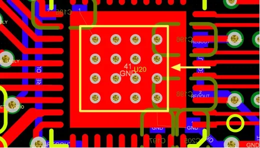
Can You Place a Via on a Pad?

PCB Design for UAV Flight Controllers, ESCs, and RF Links
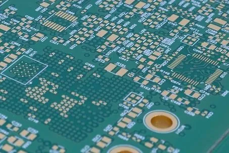
HDI PCB Design: Overcoming Challenges in High-Density Interconnect
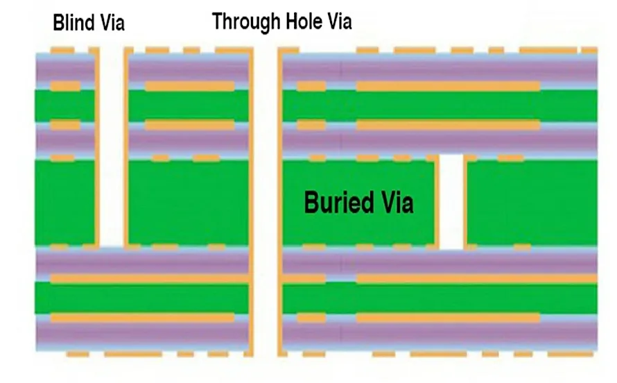
The Art of Blind and Buried Vias in High-Density Ultrasound PCBs

Mastering Hand-Soldering on Blind Via PCBs: A Hobbyist's Guide
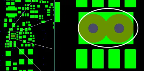
8-Layer FR-4 PCB with Blind Vias: Solder Mask Openings, Via Plugging and V-CUT Clearance Issues During CAM Review
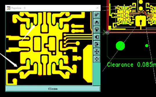
How We Resolved Stackup Warpage, Blind Via Spacing & No-Mask Conflicts in Hybrid Rogers RF PCB
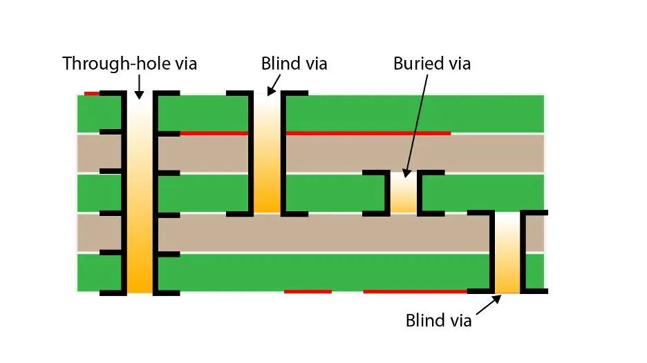
PCB Design Using Blind or Buried Vias Could Lower Fabrication Costs
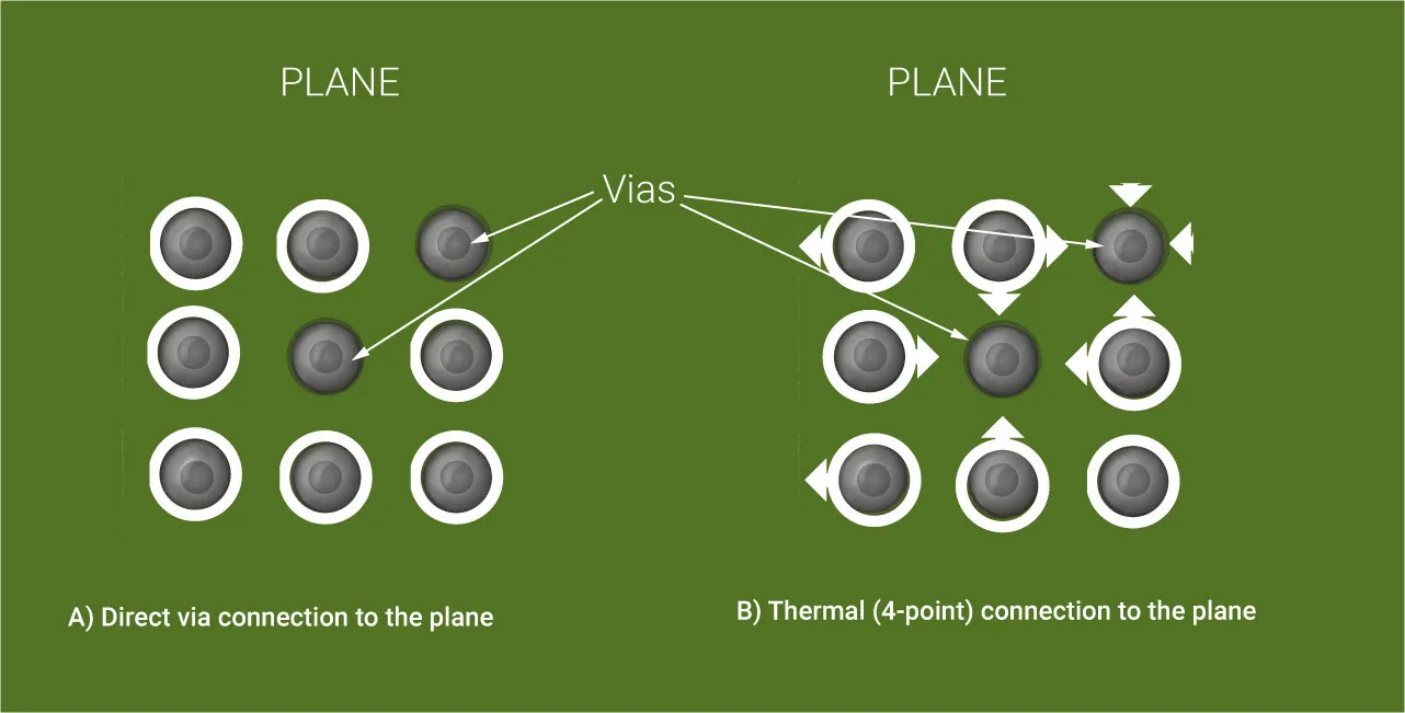
BGA Breakout Cost Optimization: Balancing Performance and Manufacturing Costs
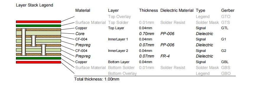
Advanced PCB Materials: Enhancing Blind and Buried Via Performance
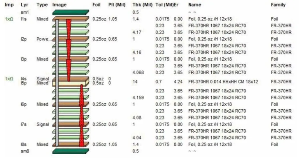
Blind and Buried Vias in Sequential Build Up PCBs: Design and Fabrication Techniques
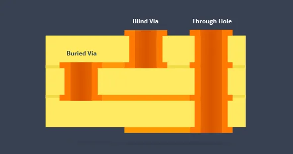
Via Technology in PCB Manufacturing: Types, Design Rules, and Optimization Techniques
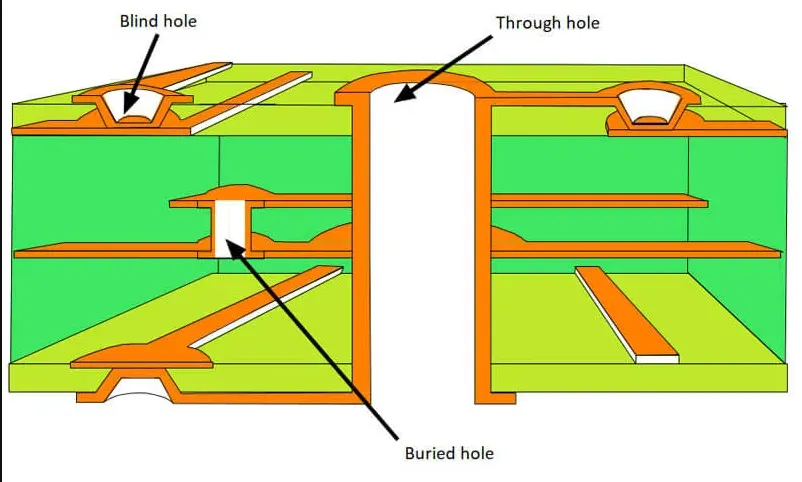
Mastering Via Design in Multilayer PCBs: A Comprehensive Guide
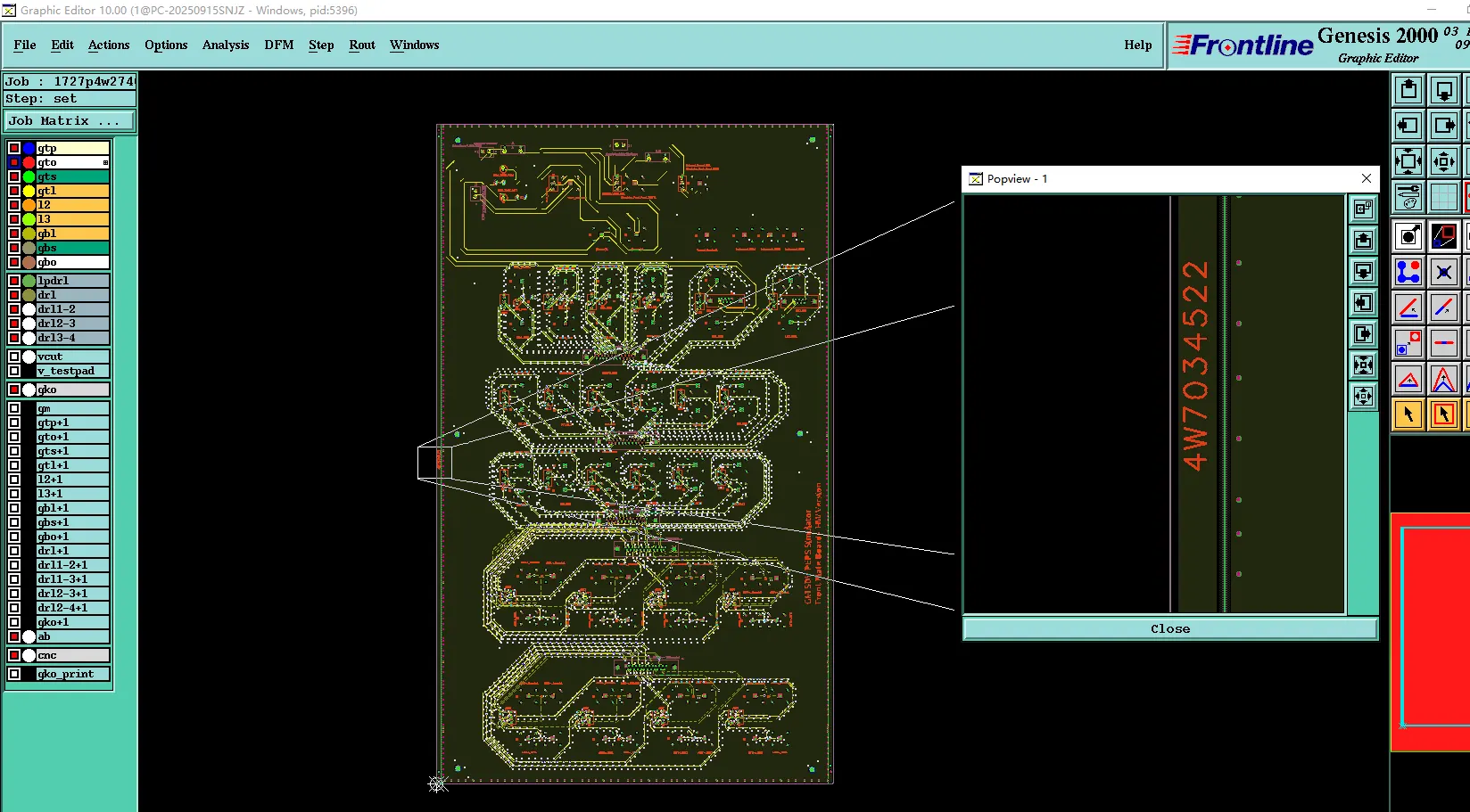
Engineering Case Study: 4-Layer FR-4 PCB Blind Via Optimization and Multi-Layer Drill Overlap Resolution During CAM Review
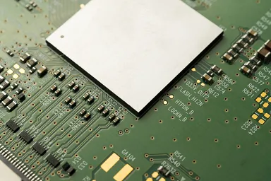
How to Choose the Right Blind Via Diameter for HDI PCB
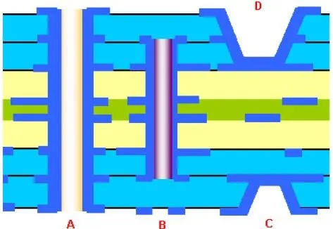
High Reliability Blind Via Design: Meeting Stringent Industry Standards
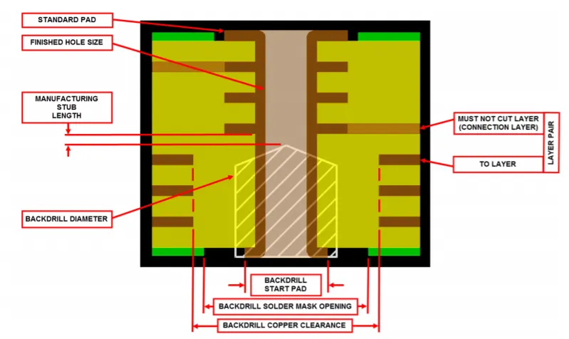
Backdrilling and Blind Vias: A Combined Approach to Signal Integrity
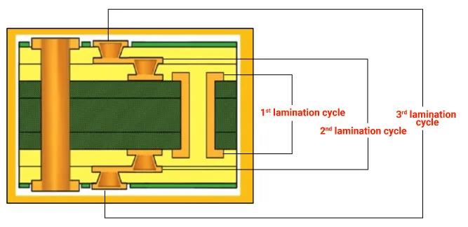
Blind and Buried Vias in HDI PCBs: Design & Manufacturing Guide