Introduction
Blind and buried vias represent critical interconnect structures in high-density interconnect (HDI) printed circuit boards, enabling denser routing and smaller form factors essential for modern electronics. These vias connect specific layers without penetrating the entire board stackup, which reduces parasitic inductance and capacitance compared to through-hole vias. However, their reliability and electrical performance are profoundly influenced by the surrounding PCB materials. High-performance PCB materials, including low-loss dielectrics and thermal management materials, address challenges like signal integrity degradation, thermal hotspots, and mechanical stress during fabrication and operation. Proper material selection for HDI ensures vias withstand laser drilling, plating, and thermal cycling without failure. This article delves into the technical principles, best practices, and CTE considerations that guide engineers in optimizing blind and buried via performance.
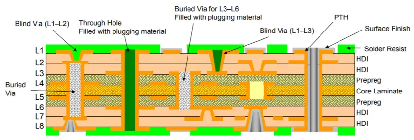
Understanding Blind and Buried Vias in HDI PCBs
Blind vias connect an outer layer to an adjacent inner layer, while buried vias interconnect two or more internal layers without reaching the surface. As outlined in IPC-2226A, these structures are classified within HDI types, such as Type II for blind vias or Type III for stacked microvias incorporating both blind and buried configurations. Their implementation allows for finer pitch components and multilayer routing efficiency, but demands precise control over via aspect ratios and fill processes. Material properties directly impact via formation, as sequential lamination requires dielectrics compatible with laser ablation or mechanical drilling. In high-speed applications, blind vias must maintain low insertion loss, while buried vias support power distribution with minimal thermal resistance. Engineers must evaluate these vias' role in overall board density before selecting materials.
The distinction between blind and buried vias influences stackup design, where buried vias enable core layers to handle high-current paths isolated from signals. Poor material choice can lead to via barrel cracking or delamination under thermal stress. HDI boards often employ multiple blind via layers, amplifying the need for uniform dielectric thickness. Standards like IPC-2226A provide guidelines on via sizing, typically recommending diameters of 150 micrometers or less for microvias. These specifications ensure compatibility with high-layer-count builds exceeding eight layers.
Key Material Properties Affecting Via Performance
High-performance PCB materials are characterized by low dielectric constant (Dk) and dissipation factor (Df) to preserve signal quality through blind and buried vias. Low-loss dielectrics minimize attenuation in high-frequency signals propagating near via stubs, which act as transmission line discontinuities. These materials typically feature Df values optimized for frequencies above 10 GHz, reducing energy dissipation as heat. In HDI designs, thin dielectric layers between via-connected layers benefit from such properties, enabling tighter coupling and lower crosstalk. Engineers prioritize these for RF and 5G applications where via performance dictates overall board efficacy.
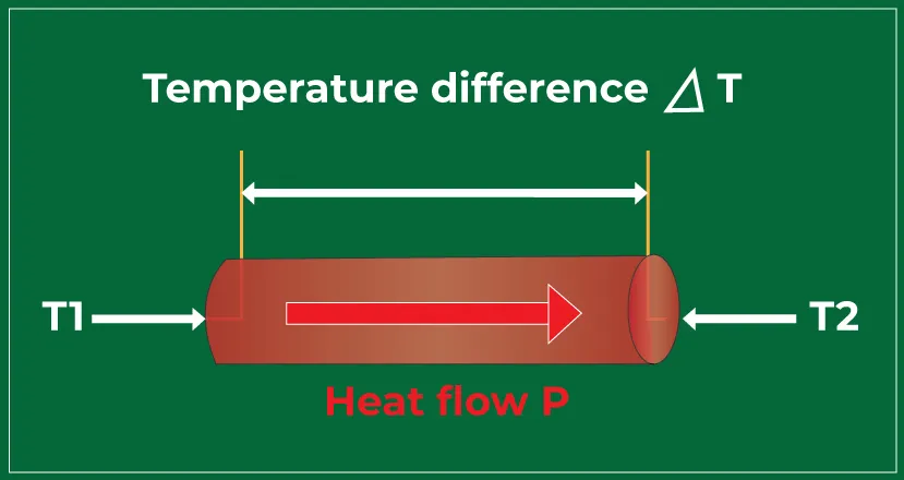
Thermal management materials enhance heat dissipation from vias carrying power or handling component hotspots. Vias serve as thermal conduits, transferring heat between layers, so materials with higher in-plane thermal conductivity improve spreading. Filled vias, common in buried structures, rely on resin systems that maintain conductivity post-cure. Low-loss dielectrics often pair with ceramic fillers to balance electrical isolation and thermal paths. This synergy prevents via overheating, which could degrade plating integrity or adjacent traces.
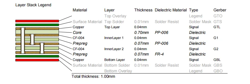
CTE considerations are paramount for via reliability, as mismatches between copper (17 ppm/°C) and dielectric z-axis CTE cause interfacial stresses. Materials with z-axis CTE below 50 ppm/°C from -55°C to 125°C reduce cracking risks during thermal excursions. IPC-4101E specifies slash sheets categorizing materials by CTE, Tg, and Td for multilayer suitability. In blind vias, where plating interfaces multiple layers, symmetric CTE across the stackup minimizes warpage. Buried vias in inner cores demand even tighter matching to prevent barrel separation under solder reflow.
Mechanisms of Performance Degradation and Material Mitigation
Signal integrity in blind vias suffers from dielectric losses and via resonance, exacerbated by higher Df materials. Low-loss dielectrics suppress these effects by maintaining phase stability and impedance control. Fabricated HDI boards reveal that via stubs shorter than quarter-wavelength at operating frequencies still induce reflections if Df exceeds thresholds. Thermal management materials counteract joule heating in high-current buried vias, preserving plating adhesion. Engineers model these using field solvers to predict insertion loss tied to material parameters.
Mechanical failures like via pullout or cratering stem from CTE-induced shear stresses during lamination or assembly. Low CTE materials distribute strains evenly, enhancing cycle life per thermal shock tests. Laser-drillable dielectrics with consistent ablation rates prevent taper issues in blind vias. For stacked vias, material uniformity across build-up layers ensures planar surfaces for subsequent processing.
Fabrication stresses, including plasma cleaning and plating, interact with material moisture absorption. High-performance materials with low moisture regain resist hydrolysis, maintaining via wall integrity. IPC-6012E qualification tests verify these under accelerated conditions, simulating field use.
Best Practices for Material Selection in HDI Designs
Material selection for HDI begins with defining electrical, thermal, and mechanical requirements aligned with application frequencies and power densities. Prioritize low-loss dielectrics for signal layers with blind vias, selecting those qualified under IPC-4101E for laser processability. Thermal management materials suit power planes incorporating buried vias, favoring high kappa prepregs. Balance cost by using hybrid stackups: standard cores for buried vias and advanced build-ups for surface blind vias.
CTE considerations guide symmetric stackups, matching outer and inner layers to control bow and twist below 0.75%. Simulate CTE mismatches using vendor datasheets to predict via stress. Validate with test coupons measuring warpage per IPC-TM-650 methods.
Optimize via fill for buried structures using conductive epoxies compatible with low CTE dielectrics, enhancing thermal paths. Sequential build processes benefit from resin-coated copper (RCC) foils as low-loss dielectrics. Prototype HDI panels to assess via chain continuity post-reliability tests.
Challenges in Advanced Material Integration
Integrating high-performance materials poses challenges like higher costs and processing sensitivities. Low-loss dielectrics often require adjusted lamination pressures to avoid voids around blind vias. Thermal management materials may increase board weight, necessitating CTE-balanced hybrids. Engineers address these through design for manufacturability (DFM), staggering via locations per IPC-2226A.
Reliability testing reveals electromigration risks in plated blind vias under high currents, mitigated by thicker copper and thermal vias. CTE-driven warpage in thin HDI panels demands fixture-controlled assembly.
Conclusion
Advanced PCB materials significantly enhance blind and buried via performance in HDI designs by addressing signal loss, thermal bottlenecks, and mechanical vulnerabilities. Low-loss dielectrics preserve high-speed integrity, thermal management materials enable efficient heat transfer, and CTE-optimized selections ensure long-term reliability. Guided by standards like IPC-2226A and IPC-4101E, engineers can systematically select materials for demanding applications. Implementing these practices yields robust boards with superior density and performance. Future advancements in nanofilled resins promise even lower losses and better CTE control.
FAQs
Q1: What role do low-loss dielectrics play in blind via performance for HDI PCBs?
A1: Low-loss dielectrics reduce dissipation factor and dielectric constant effects, minimizing signal attenuation and reflections in blind vias. They support high-frequency operation by preserving waveform integrity through shorter via stubs. In material selection for HDI, these enable tighter spacing without crosstalk penalties. Factory insights confirm their compatibility with laser drilling maintains via geometry precision.
Q2: How do CTE considerations impact buried via reliability?
A2: CTE mismatches between copper and dielectrics induce stresses leading to barrel cracks in buried vias during thermal cycling. Selecting materials with matched z-axis CTE per IPC-4101E prevents delamination in multilayer stackups. Thermal management materials further aid by distributing heat evenly. Engineers verify via chains post-stress tests for assurance.
Q3: Why are thermal management materials essential for high-performance PCB materials in HDI?
A3: Thermal management materials improve via thermal conductivity, dissipating heat from power buried vias and hotspots. They complement low-loss dielectrics by preventing performance degradation from elevated temperatures. In HDI designs, they support dense component placement without thermal runaway. Best practices include via-in-pad for enhanced spreading.
Q4: What factors guide material selection for HDI with blind and buried vias?
A4: Key factors include Df for signals, CTE for reliability, and thermal conductivity for power. High-performance PCB materials must align with IPC-2226A for via types and densities. Laser compatibility and Tg ensure process yields. Procurement teams evaluate slash sheets for balanced properties.
References
IPC-2226A — Sectional Design Standard for High Density Interconnect (HDI) Printed Boards. IPC, 2017
IPC-4101E — Specification for Base Materials for Rigid and Multilayer Printed Boards. IPC, 2017
IPC-6012E — Qualification and Performance Specification for Rigid Printed Boards. IPC, 2017


