During CAM review of a high-frequency 2-layer Rogers RO4350B board measuring 103.93 mm by 43.99 mm, our engineering team identified multiple vias positioned too close to the board edge. This via to edge clearance shortfall immediately raised the risk of hole breakout and exposed copper after V-cut and contour routing. From a DFM perspective, the primary concern was manufacturing stability and long-term via reliability rather than simple fabricability. Without clarification, the finished panels could have entered production with broken holes or edge defects that compromise both electrical continuity and mechanical integrity.
The order ( #ROG-20260321-048 ) specified Rogers RO4350B material, 0.762 mm thickness, 1 oz copper on both sides, green solder mask, black silkscreen, immersion gold finish at 1 µin, customer-panelized 1×5 array with V-cut separation, 4 mm process edge on all sides, and a nine-day delivery window. Quantity was 25 pieces in 5 sets. These parameters are typical for a compact high-frequency design, yet the combination of thin dielectric, V-cut processing, and tight via-to-edge distances required explicit engineering confirmation before release.
Why Via Placement Near the Board Edge Triggered Detailed Clearance Review
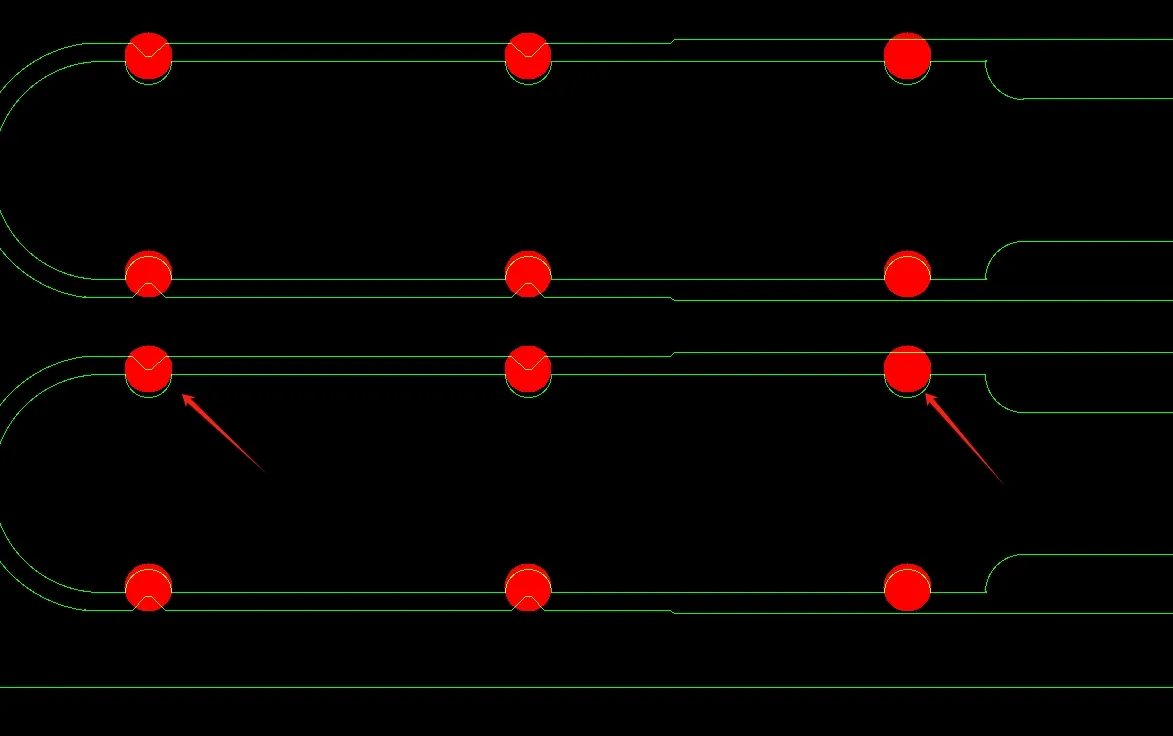
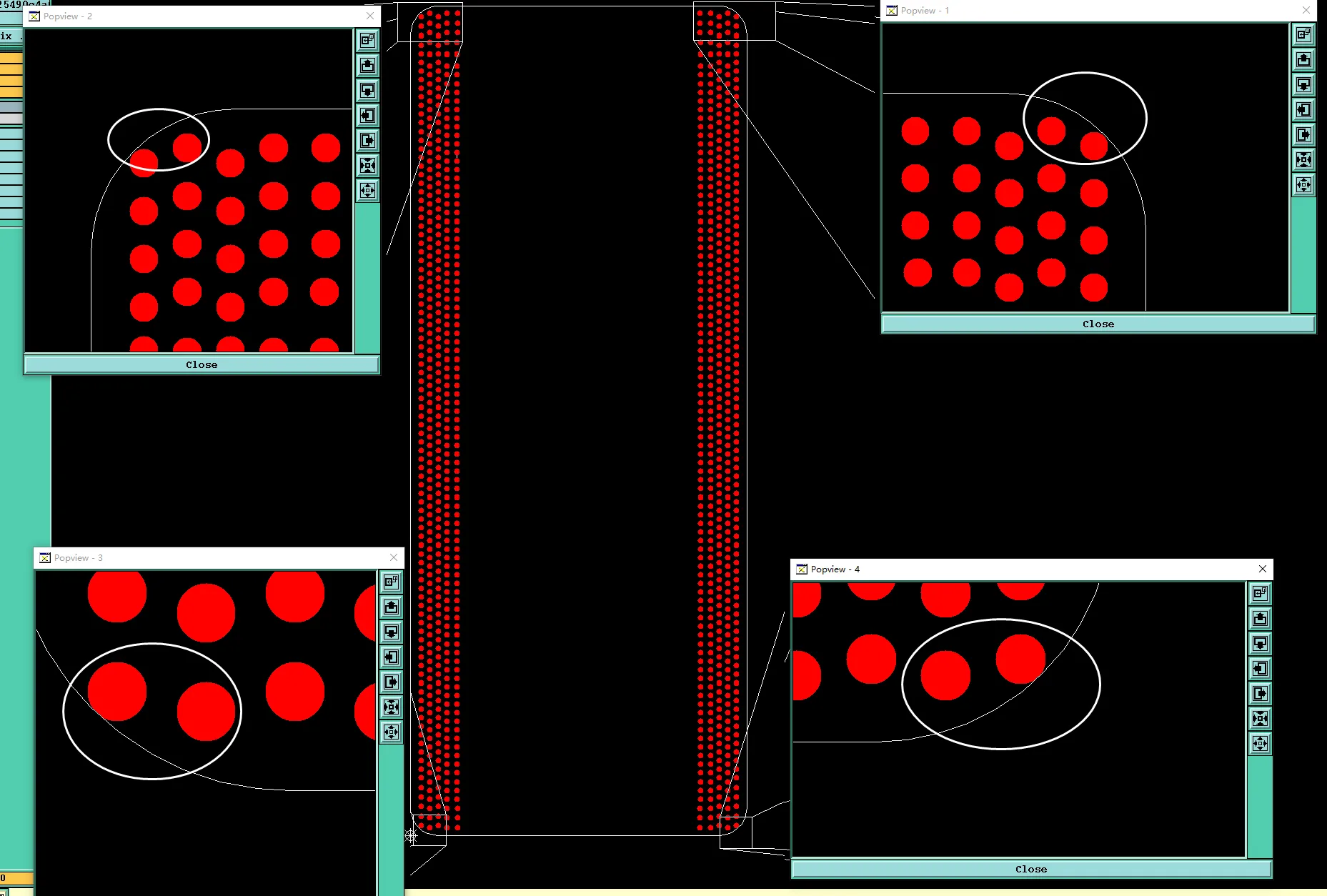
Our CAM engineer first measured the distance between the outer vias and the defined board outline against the V-cut and routing tool paths. Several vias sat inside the minimum clearance zone required for reliable edge processing on 0.762 mm Rogers material. When a via approaches the edge too closely, the V-cut blade or contour router can intersect the plated barrel, producing a broken hole, exposed copper, or reduced annular ring that fails visual and electrical inspection.
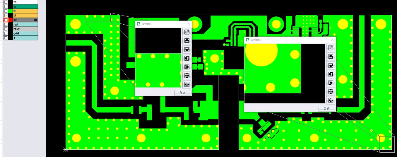
Figure 1: the via holes are too close to the board edge
Additional observations included copper features and pads also near the outline, an unusually tight finished-thickness tolerance, characters printed on large immersion-gold areas, and a paste-layer window that did not match the circuit pads. These secondary items added complexity, but the via to edge clearance issue carried the highest immediate risk of yield loss and scrap.
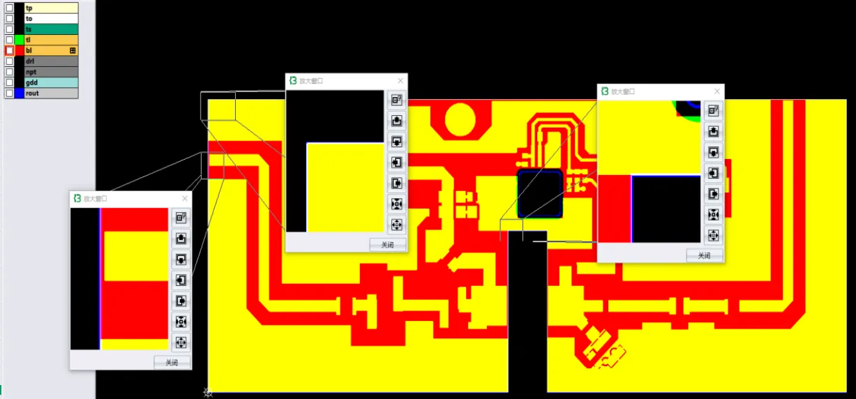
Figure 2: the pads and copper are too close to the board outline
Risk indicators included the thin 0.762 mm core, the use of V-cut without additional routing clearance, the 4 mm process edge that still left limited margin after scoring, and the high-frequency material’s known sensitivity to edge defects. On Rogers RO4350B the combination of low dielectric loss and mechanical stiffness makes any edge anomaly more critical for both signal integrity and long-term reliability.
| Feature Observed | Measured Condition | Primary DFM Risk |
|---|---|---|
| Via-to-edge distance | Insufficient on multiple locations | Hole breakout and exposed copper |
| Copper-to-outline clearance | Below safe trim allowance | Edge copper exposure after V-cut |
| Finished thickness tolerance | Tighter than process capability | Potential yield loss on thickness |
Table 1 summarizes the key observations that generated the Engineering Question.
Via to Edge Clearance and Related Edge Risks Identified During Review
The dominant risk was via to edge clearance insufficient for safe V-cut and contour processing. Manufacturing the vias in their original locations would have allowed the cutting tool to intersect the plated barrels, resulting in broken holes or copper exposure along the board edge. A second risk involved copper features and pads lying too close to the outline; after V-cut the remaining copper could be left exposed, violating typical edge-quality expectations. A third observation concerned the finished-thickness tolerance, which was tighter than the practical process window for 0.762 mm Rogers material and risked unnecessary scrap.
Secondary items included characters located on large immersion-gold surfaces and a paste-layer window that did not match the circuit pads. These were noted for confirmation but did not carry the same immediate structural risk as the via and copper clearances.
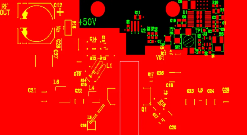
Figure 3: some characters are designed on the large gold area
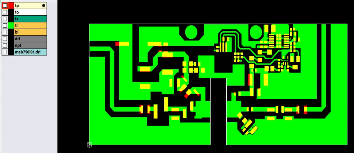
Figure 4: the solder mask opening is inconsistent with the trace pads
From a DFM perspective the priority sequence was clear: relocate the critical vias inward, decide on copper trim or acceptance of edge exposure, and adjust the thickness tolerance to a controllable range before any tooling release.
How Insufficient Via Clearance Threatens Yield and Long-Term Reliability
If production had continued without addressing the via to edge clearance shortfall, the V-cut blade would have intersected the outer vias. The result is hole breakout—partial or complete removal of the plated barrel—leaving an open circuit or a mechanically weakened via. Exposed copper along the fracture surface would then be subject to oxidation and potential dendritic growth, especially under the immersion-gold finish that does not fully cover the damaged edge.
According to IPC-A-600 acceptability criteria, broken holes and exposed copper at the board edge are classified as defects for most Class 2 and Class 3 applications. On a high-frequency Rogers RO4350B board the same defects can also introduce local impedance discontinuities and increase insertion loss, degrading signal integrity even if the board passes basic continuity testing.
Copper features left too close to the outline after V-cut create a parallel risk: residual copper that is either ragged or fully exposed. This condition can cause shorting against metal enclosures or accelerate corrosion in humid environments. The tight thickness tolerance compounds the problem by raising the probability of out-of-spec boards that must be scrapped even when electrical function is intact.
| Potential Failure Mode | Root Cause Linked to EQ | Likely Production or Field Impact |
|---|---|---|
| Hole breakout | Via too close to edge | Open circuits, scrap after V-cut |
| Exposed copper at edge | Insufficient copper-to-outline clearance | Corrosion, shorting risk, visual rejects |
| Thickness out-of-spec | Tolerance tighter than process window | Unnecessary yield loss |
| Signal discontinuity | Damaged via barrel on high-frequency board | Elevated insertion loss, field performance degradation |
Table 2 maps each realistic failure mode directly to the Engineering Question items.
Failure Scenarios the Engineering Team Sought to Prevent
Had the vias remained in their original locations, V-cut processing would have produced panels with multiple broken holes along the long edges. These boards would fail both visual inspection under IPC-A-600 and electrical continuity testing, generating immediate scrap. Even if a partially damaged via passed initial test, the reduced copper thickness in the barrel would increase the risk of via cracking under thermal cycling—especially critical on a high-frequency board that may experience rapid temperature changes in its end application.
Copper left too close to the outline after V-cut would have created ragged or fully exposed edges. In a metal enclosure these edges can short to ground or to adjacent boards, while in open environments the exposed copper accelerates oxidation and potential dendritic growth. The combination of broken vias and exposed copper would have forced a complete panel respin under the nine-day delivery window, delaying the entire program.
An unadjusted thickness tolerance would have compounded the problem by rejecting otherwise functional boards that measured slightly outside the original tight window, further eroding yield without improving product performance.
Preventive Actions Confirmed During the DFM Exchange
Our engineering team issued a focused Engineering Question that prioritized the via to edge clearance issue. The recommendation was to move the affected vias slightly inward so that the plated barrels remained fully inside the final board edge after V-cut and contour. The customer accepted this adjustment and authorized manufacture with the vias relocated inside the safe clearance zone.
For the copper-to-outline condition the team presented two clear options: accept limited exposed copper at the edge, or apply a controlled copper trim (0.33 mm from the outline in V-cut areas and 0.20 mm in routing areas). The customer selected the no-exposed-copper path with the specified trim distances, restoring edge integrity without altering functional circuitry.
The finished-thickness tolerance was revised to a practical 0.88 ± 0.10 mm window that aligns with Rogers RO4350B process capability while still meeting the Rogers PCB design intent. Characters located on large immersion-gold surfaces were confirmed to remain as designed, and the paste-layer mismatch was resolved by treating the circuit-layer pads as the governing geometry and ignoring the steel-mesh layer for fabrication purposes.
With these decisions locked, the panel drawing was verified, the CAM files updated, and the order released under the agreed nine-day schedule. The revised design retained all electrical functionality while eliminating the structural risks associated with edge proximity.
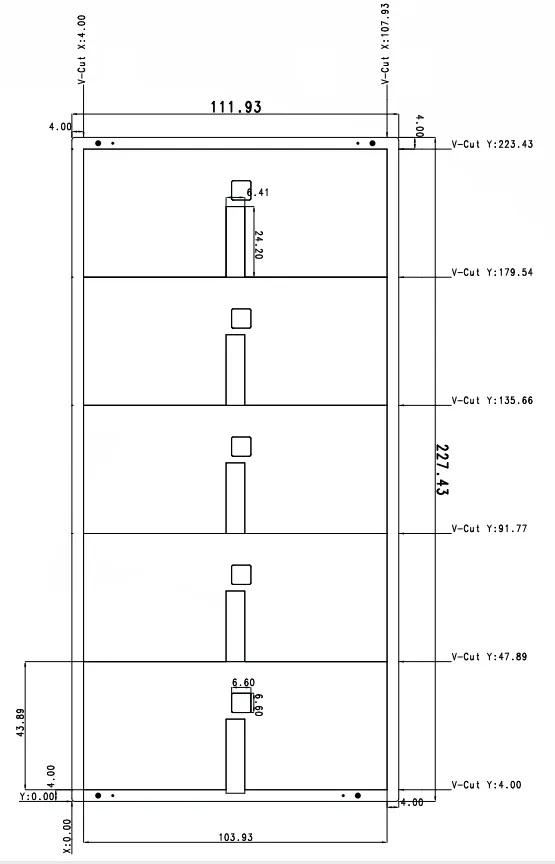
Figure 5: our panelization drawing
| Action Item | Customer Decision | Manufacturing Benefit |
|---|---|---|
| Via-to-edge clearance | Move vias slightly inward | No hole breakout after V-cut |
| Copper-to-outline | Trim copper 0.33/0.20 mm, no exposure | Clean board edges, reduced corrosion risk |
| Thickness tolerance | 0.88 ± 0.10 mm accepted | Improved yield without functional compromise |
Table 3 records the closed-loop decisions that converted an edge-risk design into a manufacturable high-frequency panel.
Building Trust Through Early Edge-Clearance Verification
This case illustrates why via to edge clearance must be treated as a first-order DFM checkpoint on thin high-frequency boards processed with V-cut. On 0.762 mm Rogers RO4350B the combination of mechanical stiffness and electrical sensitivity makes even modest clearance shortfalls capable of producing broken holes, exposed copper, and signal degradation. By identifying the issue during CAM review and obtaining explicit customer approval to relocate the vias and trim the copper, the engineering team protected both yield and long-term reliability.
Designers working with Rogers or similar high-frequency materials are encouraged to maintain adequate via-to-edge and copper-to-outline clearances in the original layout, declare thickness tolerances that align with material capability, and request early DFM feedback on panelization and edge features. These practices convert potential manufacturing problems into controlled, documented decisions before production begins.
Proactive clearance verification remains one of the highest-leverage actions a DFM team can take to safeguard both first-pass yield and field performance on high-frequency PCBs.
FAQ
Q1: Why is via to edge clearance especially critical on thin Rogers boards?
A1: Thin cores leave little material between the via barrel and the edge. When V-cut or contour tools approach the via, they can easily intersect the plating, producing broken holes or exposed copper that degrade both mechanical strength and high-frequency performance.
Q2: What realistic defects appear if vias remain too close to the board edge?
A2: Hole breakout, reduced annular ring, exposed copper, and open circuits are common. These defects fail IPC-A-600 visual criteria and can introduce local impedance discontinuities that increase insertion loss on high-frequency circuits.
Q3: How does copper-to-outline clearance interact with V-cut processing?
A3: V-cut removes a narrow strip of material along the score line. Any copper that extends into this zone is either trimmed irregularly or left exposed. Controlled pull-back of 0.20–0.33 mm restores a clean edge without sacrificing functional circuitry.
Q4: Why adjust the finished-thickness tolerance on Rogers RO4350B?
A4: Material and process variation on thin high-frequency laminates often exceeds an overly tight original window. Adopting a realistic tolerance such as 0.88 ± 0.10 mm protects yield while still meeting the design’s mechanical and electrical requirements.
Q5: Can characters printed on immersion-gold surfaces create reliability issues?
A5: In most cases they remain cosmetic if the gold surface is not a critical contact area. Confirmation that the characters may stay as designed avoids unnecessary legend edits while preserving the intended appearance.
Q6: How can designers reduce similar Engineering Questions on future high-frequency panels?
A6: Maintain adequate via-to-edge and copper-to-outline clearances in the original layout, declare thickness tolerances aligned with material capability, and request early DFM review of panelization and edge features. These steps convert potential scrap risks into controlled design decisions.