










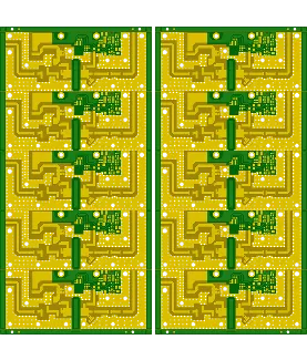
PCB Specifications
| Parameter | Value | Parameter | Value |
|---|---|---|---|
| PCB Type | Rogers PCB | Quantity | 25 pcs |
| Layers | 2 Layers | Board Type | Panel PCB |
| Dimensions | 103.93 x 43.99 mm | Copper Weight | 1oz |
| Thickness | 0.762 mm | Min Track / Spacing | 10/10mil |
| Surface Finish | ENIG (Immersion Gold) | Min Hole Size | 0.4mm |
| Solder Mask | Green | Silkscreen | Black |
| Material Type | Rogers/RO4350B |
Manufacturing Timeline
Logistics Information
Key Manufacturing Processes
Manufacturing Summary
This 2-layer Rogers board measured 103.93 × 43.99 mm with 0.762 mm thickness and used Rogers RO4350B material. Produced as 25 pieces in 1×5 panels for 5 sets, the order featured 1 oz copper, ENIG surface finish with 1 µin gold, green solder mask, and black silkscreen. Minimum holes were 0.4 mm with standard 10 mil line/space, and 4 mm process edges supported V-cut separation. The 9-day schedule included 100% flying probe testing.
DFM review resolved several dimensional and surface issues. Finished thickness tolerance was tighter than practical process control and was adjusted to a more manufacturable range after confirmation. Bottom-side circuitry was verified for full ENIG coverage. Vias located too close to the board edge risked broken holes and exposed copper; these were shifted slightly inward. Pads and copper near the outline similarly risked edge exposure after V-cut or routing; the decision followed the original design with limited copper trim (0.33 mm at V-cut, 0.20 mm at routing). Paste-layer openings mismatched the copper pads and were disregarded. Characters printed on large gold areas were retained per the original data.
Confirmed thickness control, via relocation, and edge treatments were implemented prior to production. The Rogers boards achieved consistent ENIG plating and mechanical integrity within the planned timeline. Full electrical test reports and quality certificates accompanied the shipment, confirming the panels met the high-frequency material and dimensional requirements.
Explore More PCB Manufacturing Resources
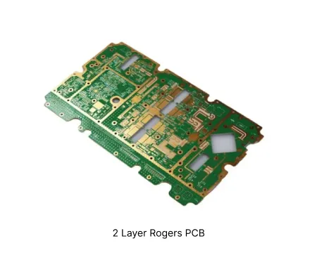
2 Layer Rogers PCB Manufacturing Insights
Discover how AIVON manufactures 2 Layer Rogers PCBs, including high-frequency material processing, dielectric performance control, RF application requirements, manufacturing challenges, and real production experience from customer orders.
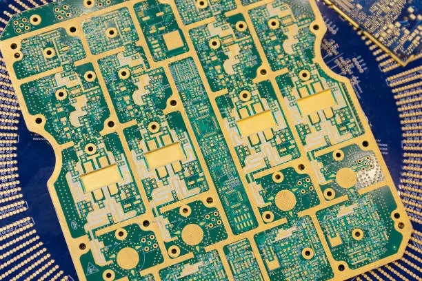
Troubleshooting Common Manufacturing Challenges with Rogers PCBs
Master troubleshooting common Rogers PCB manufacturing challenges including drilling defects, plating adhesion, delamination, and CTE mismatch. Learn practical solutions, process adjustments, and DFM tips to improve yield for high-frequency RO4000, RO4350B, and PTFE-based boards.
Real Production Records
| Order ID | PCB Type | Layers | Dimensions | Solder Mask | Surface Finish | Quantity | Action |
|---|---|---|---|---|---|---|---|
| ROG-20260527-071 | Rogers PCB | 2 | 81.7 x 81.7 | None | ENIG (Immersion Gold) | 15 | View detail |
| ROG-20260527-072 | Rogers PCB | 2 | 542.5 x 62.5 | None | ENIG (Immersion Gold) | 15 | View detail |
| ROG-20260331-041 | Rogers PCB | 2 | 51 x 165 | Green | ENIG (Immersion Gold) | 50 | View detail |


