










PCB Specifications
| Parameter | Value | Parameter | Value |
|---|---|---|---|
| PCB Type | Rogers PCB | Quantity | 50 pcs |
| Layers | 2 Layers | Board Type | Panel PCB |
| Dimensions | 51 x 165 mm | Copper Weight | 1oz |
| Thickness | 0.762 mm | Min Track / Spacing | 5/5mil |
| Surface Finish | ENIG (Immersion Gold) | Min Hole Size | 0.3mm↑ |
| Solder Mask | Green | Silkscreen | White |
| Material Type | Rogers/RO4350B |
Manufacturing Timeline
Logistics Information
Key Manufacturing Processes
Manufacturing Summary
This 2-layer high-frequency board measured 51 × 165 mm and used Rogers RO4350B material with a 0.762 mm core. Produced as 50 single pieces, the order featured 1 oz finished copper, ENIG surface finish (2 µin gold), green solder mask, and white silkscreen. Minimum holes were 0.3 mm with a tight 5 mil line/space geometry. Finished thickness was controlled to 0.9 ± 0.1 mm. The 5-day schedule included 100% flying probe testing on the customer self-panel format.
DFM review addressed material, edge, and stamp-hole constraints. The core was processed as Rogers 4350B H/H without copper cladding, with finished copper brought to 1 oz. Copper-to-outline clearances fell below the 0.2 mm single-side minimum and risked exposed or peeled copper after routing. Multiple via-in-pad features required confirmation of intent. Character orientation symbols carried solder-mask openings that needed verification. Mouse bites were initially reviewed as NPTH; after customer clarification that PTH was required, the original 0.8 mm diameter and 0.267 mm spacing were found to exceed process capability and risk board breakage. The stamp holes were therefore reduced to 0.5 mm diameter with 0.4 mm spacing to maintain panel integrity.
Confirmed thickness control, edge clearances, via-in-pad treatment, and stamp-hole geometry were implemented prior to production. The Rogers boards achieved consistent ENIG plating and mechanical stability within the accelerated timeline. Full electrical test reports and quality certificates accompanied the shipment, confirming the panels met the high-frequency material and dimensional requirements.
Explore More PCB Manufacturing Resources
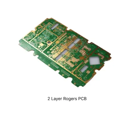
2 Layer Rogers PCB Manufacturing Insights
Discover how AIVON manufactures 2 Layer Rogers PCBs, including high-frequency material processing, dielectric performance control, RF application requirements, manufacturing challenges, and real production experience from customer orders.
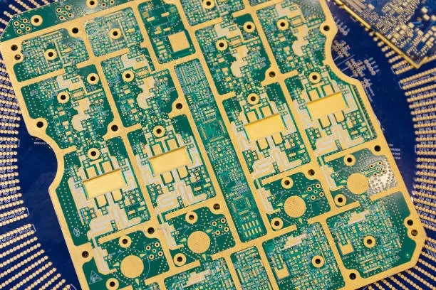
Troubleshooting Common Manufacturing Challenges with Rogers PCBs
Master troubleshooting common Rogers PCB manufacturing challenges including drilling defects, plating adhesion, delamination, and CTE mismatch. Learn practical solutions, process adjustments, and DFM tips to improve yield for high-frequency RO4000, RO4350B, and PTFE-based boards.
Real Production Records
| Order ID | PCB Type | Layers | Dimensions | Solder Mask | Surface Finish | Quantity | Action |
|---|---|---|---|---|---|---|---|
| ROG-20260527-071 | Rogers PCB | 2 | 81.7 x 81.7 | None | ENIG (Immersion Gold) | 15 | View detail |
| ROG-20260527-072 | Rogers PCB | 2 | 542.5 x 62.5 | None | ENIG (Immersion Gold) | 15 | View detail |
| ROG-20260331-008 | Rogers PCB | 2 | 86 x 57.7 | Green | ENIG (Immersion Gold) | 50 | View detail |


