 00:54
00:54
Mouse Bites
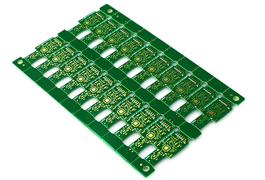
Mouse bites are a practical technique in printed circuit board (PCB) manufacturing, designed to facilitate the separation of individual boards from larger panels. These small, perforated tabs resemble tiny bite marks, hence the name, and they allow for efficient production runs by enabling multiple PCBs to be fabricated together on a single sheet. For engineers and hobbyists searching for information on mouse bites, this tag serves as a comprehensive resource, covering their design, implementation, and troubleshooting in various electronics projects. Understanding mouse bites is essential for optimizing PCB assembly processes. They provide a cost-effective alternative to v-scoring or routing, particularly in low-volume production or prototyping where minimizing material waste and simplifying depanelization are key priorities. By incorporating mouse bites, designers can ensure clean breaks without damaging traces or components, which is critical for maintaining signal integrity and board reliability. Practical applications include consumer electronics, automotive sensors, and IoT devices, where space constraints demand precise panelization methods. To achieve the best results, follow best practices such as placing mouse bites away from sensitive areas, using appropriate hole sizes (typically 0.5 to 1 mm in diameter), and testing prototypes to avoid stress fractures. This approach not only streamlines manufacturing but also reduces the risk of defects during separation. For deeper insights into integrating mouse bites with other panelization techniques or addressing common challenges like alignment issues, the articles linked under this tag offer detailed guidance based on real-world examples.
Video Guide
-
00:54
Technical Articles
Optimizing Breakaway Tabs: Minimizing Stress in PCB Depanelization
Depanelization Techniques: Stamp Holes vs. V-Scoring for PCBs
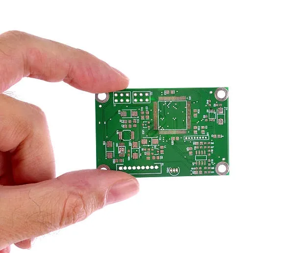
Understanding Mouse Bites: A Key to Efficient PCB Manufacturing
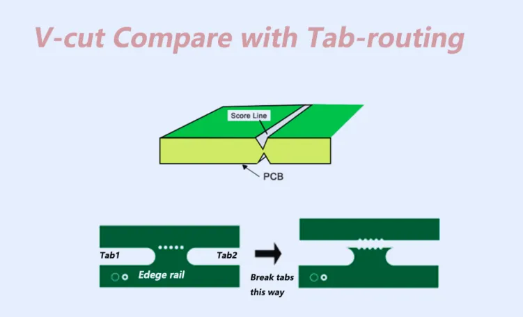
PCB Panelization: V-Cut vs. Tab-Routing for Efficient Manufacturing
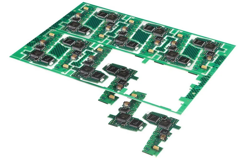
Mastering Irregular Shapes: Tab Routing for Complex PCB Panel Designs
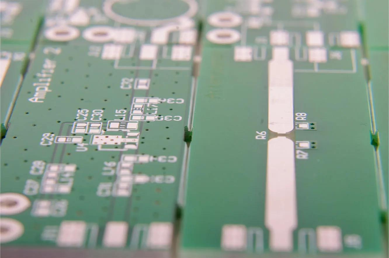
Depanelization Demystified: Mouse Bites vs. V-Score in PCB Manufacturing