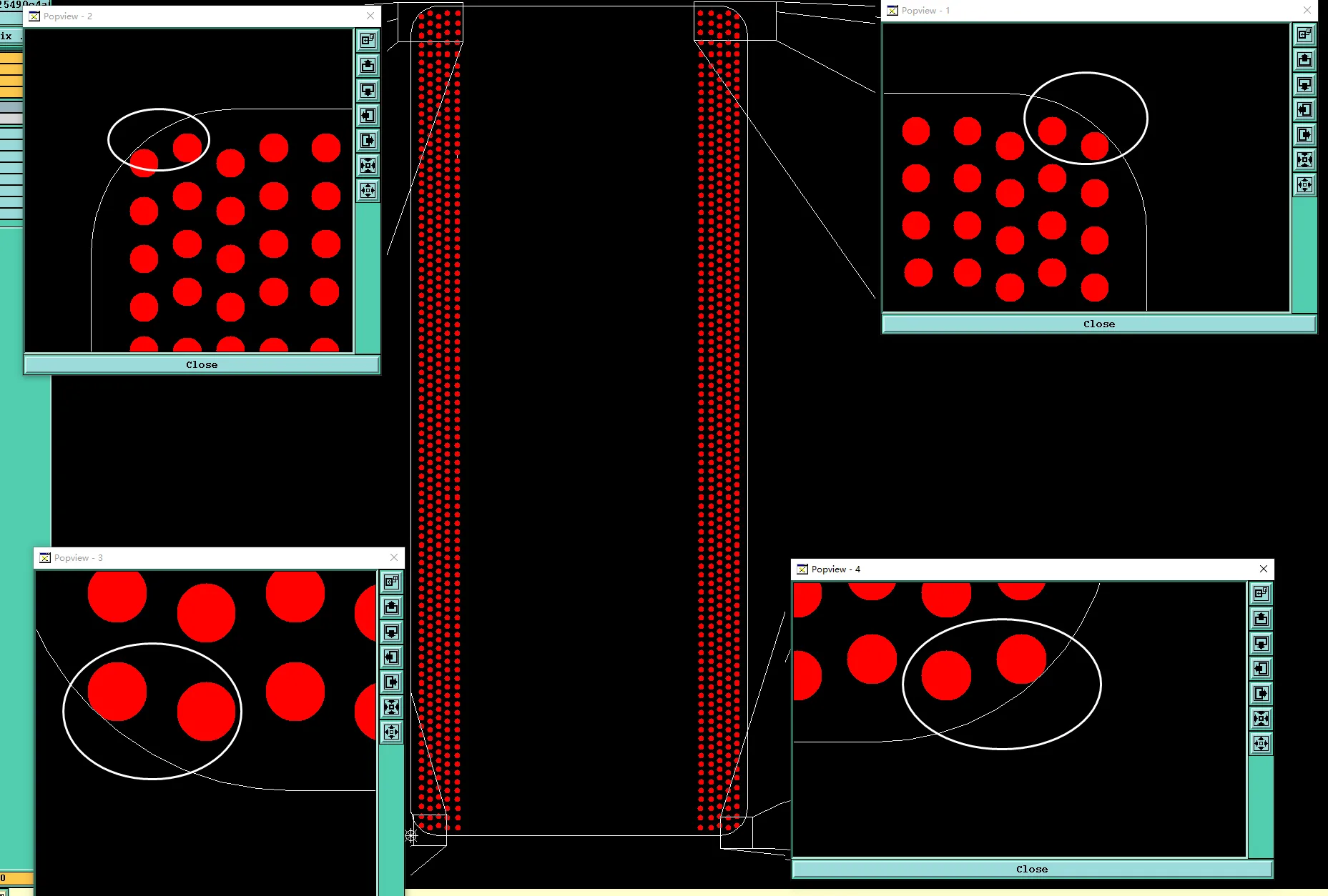
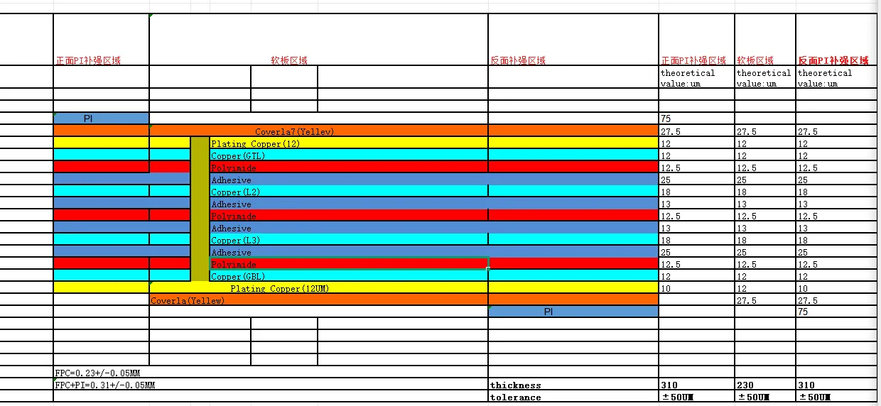
The central engineering issue recorded for this order is a direct conflict between finished thickness and copper weight on a 6-layer flexible circuit. The customer specified a board thickness of 0.23 mm together with inner copper of 0.5 oz and outer copper of 1 oz. The factory states that these two requirements cannot be met simultaneously and proposes an alternative stack-up in which inner-layer copper is controlled to 1/3 oz and finished outer copper is held between 0.6 oz and 0.8 oz. The part measures 490 × 36 mm, uses rolled copper, is laser-formed, and carries ENIG. Both sides are specified without coverlay and without silkscreen. Quantity is 60 pieces supplied as customer-panelized sets. No acceptance of the proposed copper weights, no revised stack-up drawing, and no confirmation that the production files have been updated appear in the records.
6-Layer FPC Thickness and Copper Weight Requirements
The order ( #FPC-20250117-0056 ) parameters list a finished thickness of 0.23 mm and copper weights of ½ oz Cu / 1 oz Cu. In the engineering note the factory restates the requirement as 0.23 mm thickness with 0.5 oz inner and 1 oz outer copper. For a 6-layer flexible construction the total thickness is the sum of the dielectric films, adhesive layers, and the copper foils on all six layers. Each ounce of copper contributes a nominal thickness of approximately 35 µm before plating. When six copper layers are present, even modest foil weights consume a substantial fraction of a 0.23 mm budget once the necessary polyimide and adhesive thicknesses are included to maintain layer separation and mechanical integrity.
The factory explicitly states that the specified copper weights cannot be achieved while still meeting the 0.23 mm finished thickness. No calculation of the exact shortfall is supplied, yet the statement establishes that the combination of layer count, dielectric minimums, and the requested foil weights exceeds the allowed overall thickness. The board is identified as an FPC, and the absence of coverlay on both sides further reduces the number of dielectric layers available to absorb thickness, leaving the copper foils and the core adhesive system as the dominant contributors.
Proposed 6-Layer FPC Stack-Up and Copper Weight Adjustments
In response the factory recommends that the board be built to its own stack-up. Under that proposal inner-layer copper is controlled to 1/3 oz and finished outer copper is controlled between 0.6 oz and 0.8 oz. The suggestion is presented as the means of satisfying the 0.23 mm thickness while still providing usable copper on all layers. Reducing the inner foils from 0.5 oz to 1/3 oz lowers the copper contribution on the four internal layers; limiting the outer finished copper to 0.6–0.8 oz instead of 1 oz reduces the plated thickness on the two external layers. Together these reductions are offered as the adjustment required to bring the total stack inside the specified thickness.
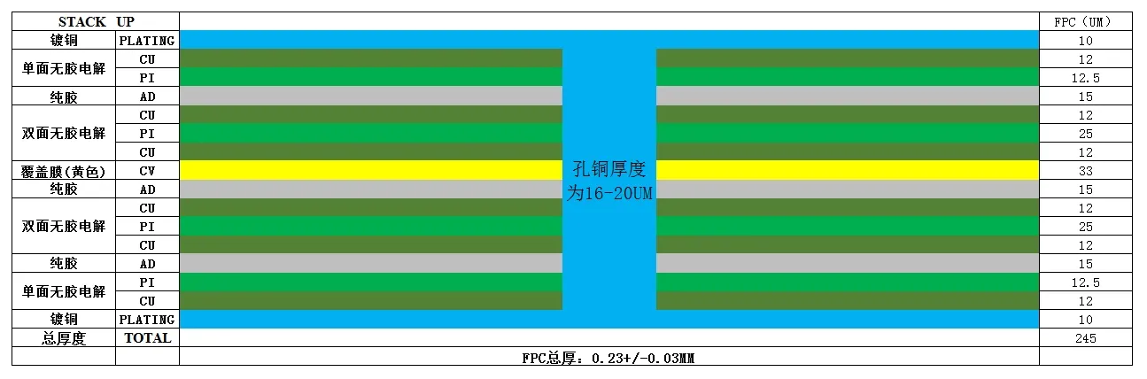
Figure 1: 6-layer FPC stack-up
The proposal remains a recommendation. The records contain no customer reply accepting the lower copper weights, no statement that the production Gerbers or stack-up drawing have been revised to the new values, and no confirmation that the 0.23 mm thickness has been verified against the proposed construction. The note ends by asking whether the production draft is acceptable, indicating that the files incorporating the suggested copper weights are still under review.
Additional FPC CAM Issues: Via Pads and NPTH Alignment
Two further observations appear in the same communication. The first concerns PTH vias of R0.5 mm for which the bottom-layer circuitry contains no via pads. The second notes that an NPTH hole layer does not align with the outline clearance. A customer remark on the order states "No NPTH drills." These items are recorded alongside the thickness discussion but are not linked to it. They indicate that the production file review also identified missing pads and a layer-to-outline mismatch, yet they do not alter the copper-weight versus thickness conflict that forms the main subject of the note. The request for production-draft confirmation encompasses all of these points.
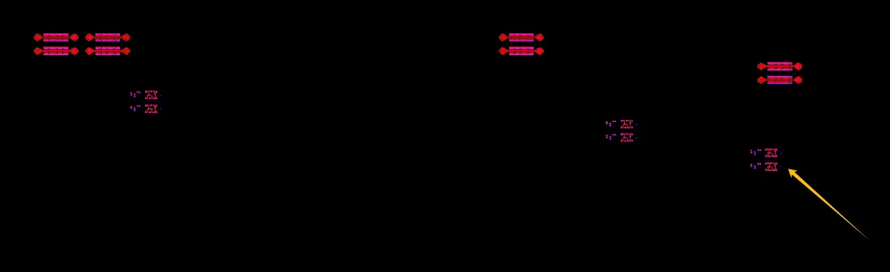
Figure 2: As shown in the picture, the arrow points to the PTH layer 0.5MM vias, there is no pad on the bottom line
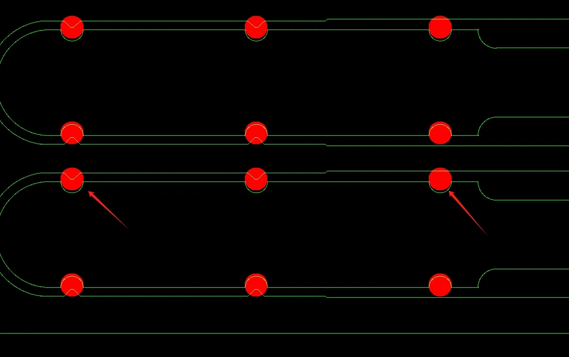
Figure 3: As shown in picture, If the NPTH layer overlaps with the outline layer as shown in the data
The order lists laser forming, ENIG of 1.00, via-cover-oil, and a 3 mil trace-and-space capability. None of these parameters is cited by the factory as a reason for the copper-weight adjustment. The adjustment is attributed solely to the impossibility of meeting both the 0.23 mm thickness and the original 0.5 oz / 1 oz copper specification on a 6-layer flexible PCB.
FPC Stack-Up Approval and Production File Confirmation
The engineering record establishes a clear sequence: the customer requirements for thickness and copper weight are restated, the conflict for a 6-layer construction is declared, and a specific alternative (1/3 oz inner, 0.6–0.8 oz finished outer) is offered. No subsequent entry indicates that the alternative has been accepted, that the copper weights have been changed in the released data, or that a thickness measurement has confirmed compliance.
Until that confirmation is recorded, the documented status is that the original 0.5 oz / 1 oz specification cannot be met at 0.23 mm and that the factory has proposed reduced copper weights as the means of resolving the conflict. The proposal addresses only the thickness and copper-weight relationship; it does not resolve the separate notes concerning missing via pads or NPTH alignment. Those items remain part of the same open production-file review.
The case therefore rests on a single, explicitly stated manufacturing constraint. On this 6-layer flexible circuit the combination of 0.23 mm finished thickness and 0.5 oz / 1 oz copper exceeds what the layer count and dielectric requirements will allow. The factory response is a concrete proposal to reduce inner copper to 1/3 oz and finished outer copper to the 0.6–0.8 oz range. No further outcome is documented.