When copper or an SMD pad sits on the board outline, PCB edge clearance is no longer a drawing note. The router or the V-cut will cut whatever occupies that line — exposed copper on the finished edge, a clipped land, or both.
This article is the CAM review of that overlay. A pour on the outline: keep the copper and accept the exposure, or confirm a factory copper shave. An SMD pad on the outline: accept copper on the board edge, or take the pad trim one EQ specified as 0.2 mm from the center of the outline line. An SMD pad on a V-cut: accept the short land after the score, or move the pad or the score. How close the geometry looks still leaves those choices in the close.
| What we saw in the files | Where the files disagree | What the EQ asked |
|---|---|---|
| Outline too close to a copper pour | The route would cut copper, so the finished edge can show metal on the cut face | Confirm a factory copper shave on that pour, or keep the copper and accept the exposure |
| SMD pad too close to the outline | Forming can cut the land or leave copper on the board edge | Keep the pads as drawn and accept edge exposure, or accept the pad trim specified as 0.2 mm from the outline-line center |
| SMD pads too close to the V-cut | The score removes copper through part of the land | Confirm the clipped land and copper on the scored face, or move the pad or the score / change forming on that edge |
PCB Edge Clearance Between the Outline and Released Copper
When a package talks about PCB edge clearance, what we have to work with is the outline file against the copper file as part of PCB panelization. SMD pad, in the EQ wording we see, means a surface-mount land. Whether that land is solder-mask-defined is a separate reading of the mask file. A forming note may say that edge will be V-cut instead of routed. An order note may mention copper on the edge, or exposure. Those notes still leave us putting the outline on the copper and looking at the hits.
The designer may have wanted the pour or the pad to run all the way to the edge. They may have thought they left a gap that the outline file does not actually leave. The two files do not tell us which of those was intended. Both are already released.
The edge in question is the finished contour of the board. Copper poured on a process-edge rail for plating or warpage belongs to that other review.
A factory copper shave, or a pad trim written as 0.2 mm from the outline-line center, is a proposal in the EQ. It is a change to copper that was already released, so it waits on a written close.
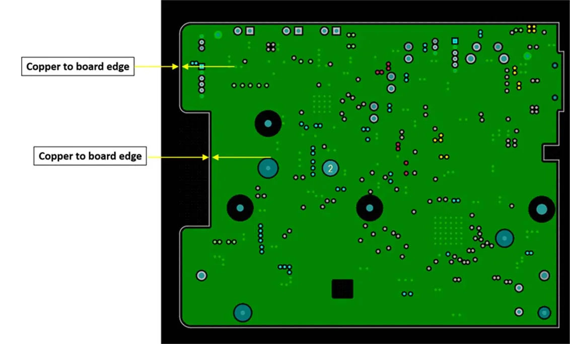
Copper-to-Edge and Pad-to-Edge Clearance on the Outline Overlay
We put the outline over the outer copper and the SMD pads. Where a V-cut will be the finished edge, we put that line on the same stack. Copper-to-edge clearance and pad-to-edge clearance are the distances that stack produces.
From it we can see how far a pour or a trace sits from the outline, how far a land sits from the outline, and whether anything touches or crosses the route or the score. We can also see which cut will form that edge — the router or the V-cut.
The stack still leaves several questions open: whether copper on that edge is acceptable, whether the land has to stay full size for solder, and whether we are being asked to pull the pour back or clip the pad. The 0.2 mm figure from the outline-line center came from one EQ. The overlay does not turn it into the remaining clearance.
A pad can miss the outline and still sit in the score. Those are two edges. We write down clear, touch, or cross at each site and which line will cut it. That record is the finding. The close is the next step.
| What the overlay shows | What still has to be confirmed |
|---|---|
| How far a pour or trace sits from the outline | Whether copper on the formed edge is acceptable |
| How far an SMD pad / land sits from the outline | Whether that land has to stay full size for solder |
| Whether copper or a land touches or crosses the route | Whether the pour may be pulled back from the outline |
| Whether a land touches or crosses the V-cut | Whether the pad may be clipped, or whether 0.2 mm from the outline-line center is the remaining clearance |
| Whether that site finishes as a routed outline or a V-cut | Which close applies when pour sites and pad sites exist on the same board |
Routed Outline Versus the V-Cut as the Finished Edge
If the package scores the array, distance to the outline is a different measurement from distance to the score. Pads that sit on the V-cut are a score-path problem. A pour or a pad that sits on the outline is an outline-path problem, unless the same site is scored as well. Before we write the EQ we name the line that will actually cut the copper.
Copper-to-Edge Clearance Too Close to the Outline
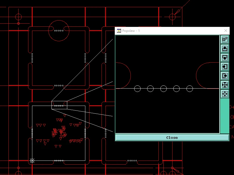
On the first job the pour ran onto the outline. Send the router through that copper and the cut face shows metal — exposed copper at the board edge, creating a PCB edge clearance concern.
The factory note offered a copper shave: pull the pour back before forming so the cut face is laminate. That edit changes copper that was already released. If the designer meant the pour to run to the edge, pulling it back is a design change, not a cleanup of leftover copper. The shave waits on the close.
This is a pour on the finished board contour. Rail width and how dense a pour sits on a process edge stay in that other review, and the EQ did not publish a shave distance as a factory default.
For each tight pour the question is the same: keep the copper as drawn and accept metal on the formed edge, or allow the factory copper shave on that pour. SMD pads on the same edge are a separate close. A land is not handled as a pour shave.
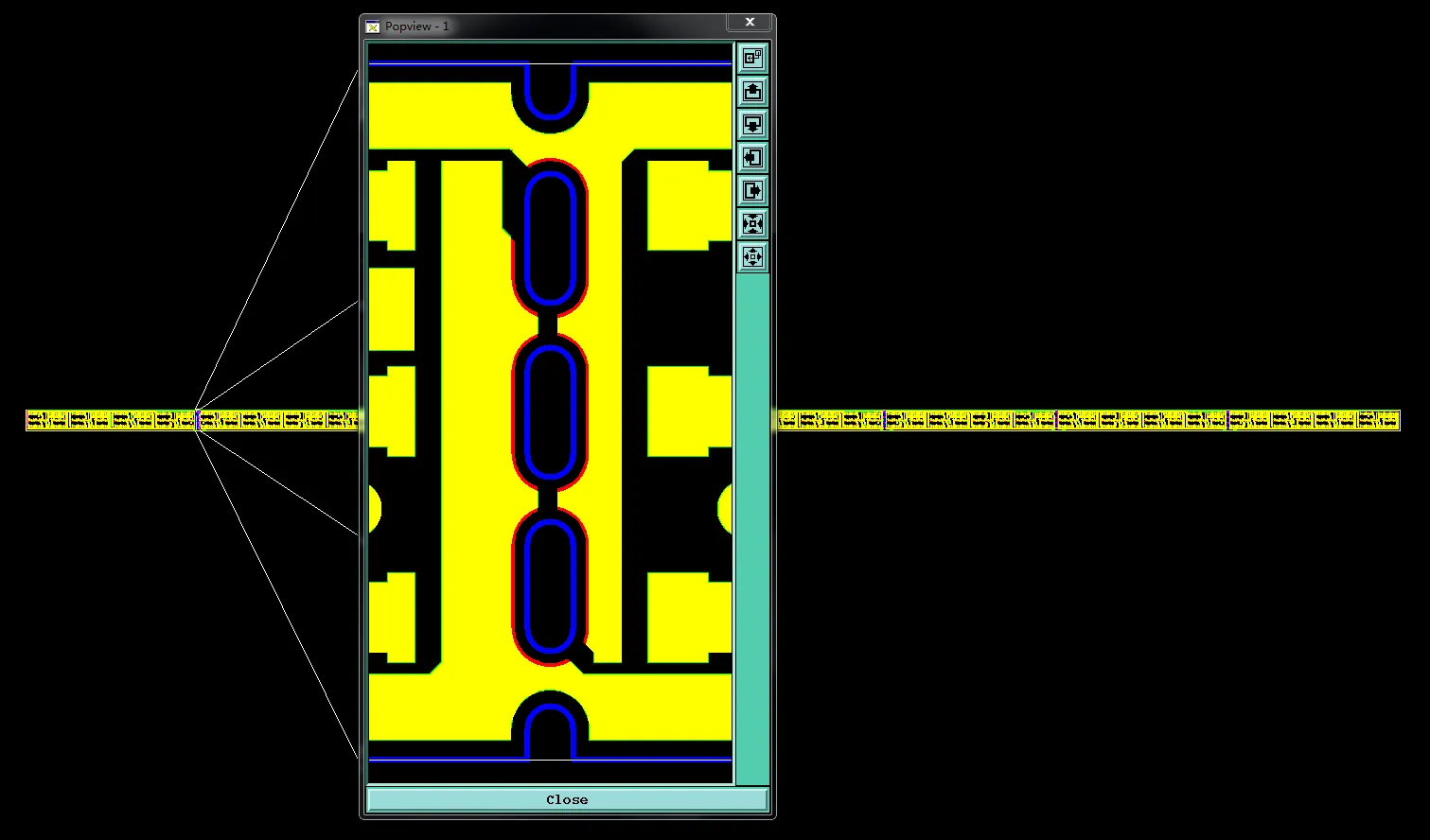
The outline is too close to the copper, to avoid the finished PCB copper exposed, we will shave the copper
SMD Pad Too Close to the PCB Edge
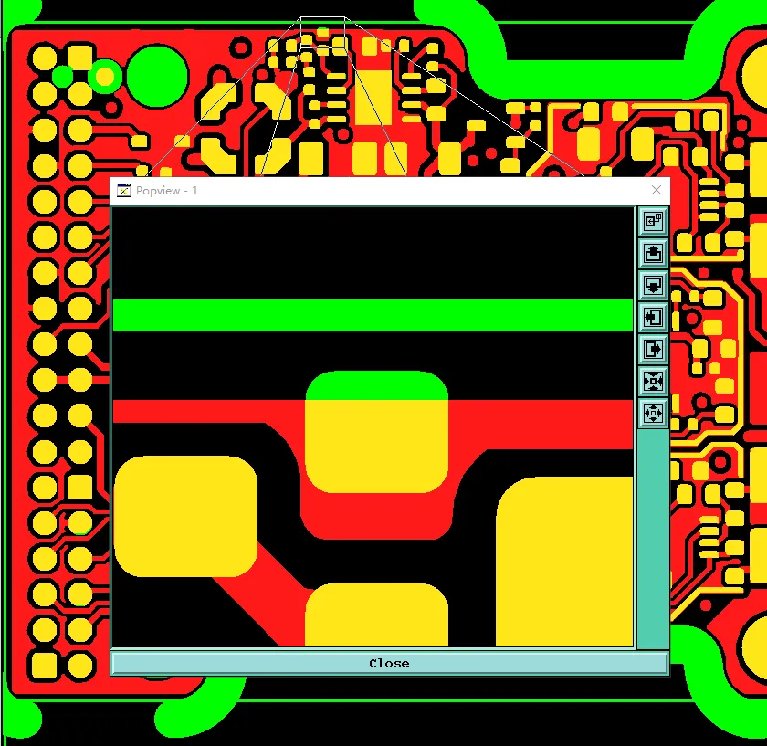
When an SMD pad sits that close to the outline, forming can take part of the land or leave copper on the edge. That is the pad against the outline, rather than the pour against the outline.
The EQ offered two suggestions. Suggestion 1 was to follow the data and accept copper on the board edge. Suggestion 2 was to trim the pad so what remains sits 0.2 mm from the center of the outline line.
That 0.2 mm is what the EQ proposed. It is a quoted value on that job, not a clearance copied onto every board. Clipping a land is also a different edit from pulling a pour back. The solderable area changes, and so does how the part sits at assembly.
Whether copper on that edge is acceptable is the customer's call. The overlay shows the occupancy; it does not classify the edge as cosmetic or electrical.
We name the lands that sit on the outline and ask: keep them and accept the exposure, take the quoted trim, or redraw the land or the outline. Unless the same site is both pour and pad, the pad close stays separate from a pour shave.
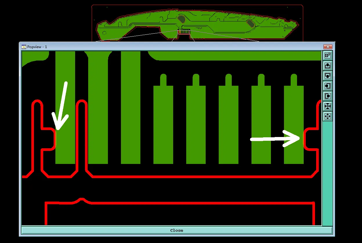
The SMD pad is too close to the board outline, which may cause copper exposure on the board edge.
SMD Pads Too Close to the V-Cut
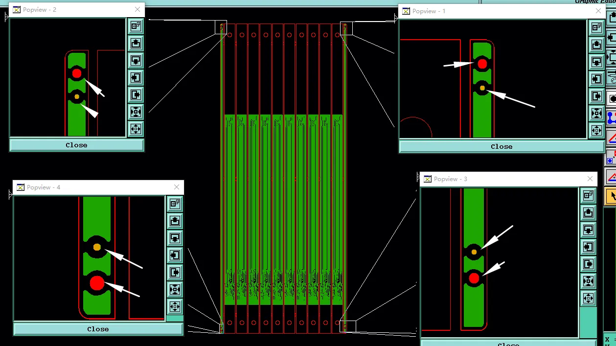
On the V-cut jobs some of the SMD pads sat on the score line. Once that plane is cut, part of the pad is gone — a short land on the finished edge and copper on the scored face.
Moving the pad, moving the V-cut, or switching that edge to a routed outline waits on the close. If the same board also has pour sitting on the outline, that stays a separate line in the EQ. A copper shave on the pour leaves the pad in the V-cut as it was.
We show which lands the score will clip, then ask whether to keep the pad and accept the short land, move the pad or the score, or change how that edge is formed. The 0.2 mm outline-center trim applies here only if the customer uses that same edit on the scored pads.
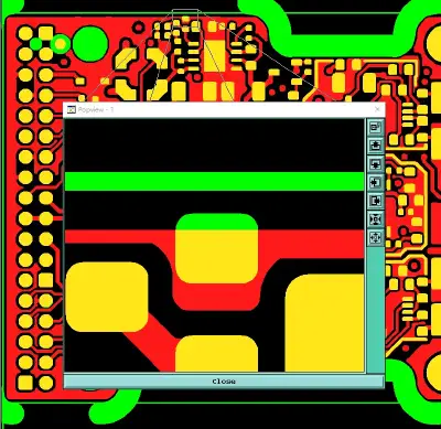
Some solder pads are positioned too close to the edge. V-CUT may cut part of pads.
Accept PCB Edge Copper Exposure or Confirm the Shave
The written close names the files and the sites. Cosmetic versus electrical is not something we assign from the overlay. On a mixed board the answers can differ by site: shave a pour on one edge, accept exposure on a pad, move a pad off a V-cut.
| Path | What stays as drawn | What the close allows us to change | What the finished edge will be |
|---|---|---|---|
| Keep the artwork | Outline, copper, pads, and V-cut as released | No shave, no pad trim | The customer accepts copper on the edge and, where the overlay already shows it, a clipped land |
| Accept the factory copper shave | Outline and pads, unless a pad site is also named | Pull the pour back from the formed edge as proposed in the EQ | The pour no longer sits in the route or the score; this is not a pad redesign |
| Accept a pad trim or a new location | Outline and V-cut, unless the customer also moves them | Trim the named SMD pads — quoting 0.2 mm from the outline-line center only if that suggestion is accepted — or place a revised pad or score | The land stays a solderable feature, or the score no longer cuts it |
Before the package goes out, put the outline and the V-cut on the outer copper and the SMD pads. If something crosses the cut, write keep, accept-exposure, shave, or trim into the note. Leaving that choice out of the package is how the EQ starts. Until that line is written, copper and lands stay as released.
PCB Edge Clearance Questions From CAM Review
Q1: What is PCB edge clearance?
A1: On our desk it is the gap we measure when the board outline — or the V-cut, when that score is the finished edge — is laid on the outer copper and the SMD pads. The package does not give us a separate file for it, and this review does not publish a factory table of values.
Q2: What is PCB copper-to-edge clearance?
A2: How far a pour or a trace sits from the line that will form the board. When that distance runs out, the router or the score can leave copper on the cut face. Whether that copper is allowed is the close, rather than the measurement itself.
Q3: What is PCB pad-to-edge clearance?
A3: The same overlay, this time against an SMD pad rather than a pour. A land can miss the outline and still sit in a V-cut, so we record the two edges separately.
Q4: What happens when an SMD pad is too close to the PCB edge?
A4: Forming can cut the land or leave copper on the board edge. One EQ on that condition offered two closes: keep the pads as drawn and accept the exposure, or trim the pad so the remaining land sits 0.2 mm from the center of the outline line. That 0.2 mm figure is the proposal written in that EQ.
Q5: What is PCB edge copper exposure?
A5: Copper you can see on the formed edge after routing or V-cut, because a pour or a land was sitting in the cut. The overlay shows that. Whether to live with it is the customer's decision on the named site.
Q6: Is a copper shave the same as trimming an SMD pad?
A6: They are different edits. A copper shave pulls a pour back from the formed edge. A pad trim changes a solderable land. A pour shave leaves an SMD pad as it was. The quoted 0.2 mm outline-center trim becomes the V-cut close only if the customer applies that edit to the scored pads.
Q7: Does clearing the outline mean an SMD pad also clears a V-cut?
A7: Distance to the outline is a different measurement from distance to the score. Pads that sit on the V-cut are still in the cut even when they miss the outline file. We name the line that will cut the copper before we write the close.