Aluminum base PCBs present unique manufacturability challenges compared to standard FR-4 boards. This engineering case examines a real 1-layer aluminum PCB order that required multiple engineering questions during CAM review. As a senior CAM engineer, I frequently encounter issues related to aluminum's hardness, thermal material constraints, and mechanical processing limitations.
With 3.0W/m·K thermal conductivity, 1.0mm thickness, and high voltage testing requirements, this project highlighted several critical DFM concerns. This article details the issues discovered, manufacturing risks involved, and how timely clarification ensured successful production.
Order Overview
This was a single-layer aluminum PCB ( #ALU-20260120-012 ) using TG130 material from Guangdong Boyi with 3.0W thermal conductivity. Board thickness was 1.0mm with 1oz copper. Minimum hole size was 1.5mm and line/space 10mil. Surface finish was OSP, with black silkscreen and no solder mask on the bottom. The order required 100% AOI inspection and 100% AC3000V high voltage testing. Panelization was 1x6 with V-cut scoring. Quantity was 30 pieces.
Special requirements included custom slot milling and tight process controls for thermal performance. While single-layer aluminum boards are generally straightforward, the combination of small slot features, edge proximity, and material availability created several production hurdles that needed customer confirmation.
Main Engineering Questions Found During CAM Review
Slot Width Machining Limitation on Aluminum
The customer designed slots at 1.0mm width, but aluminum substrate is significantly harder than FR-4. Our milling tools could not reliably produce such narrow slots without risk of tool breakage or inconsistent dimensions. We proposed enlarging the slots to 1.2mm.
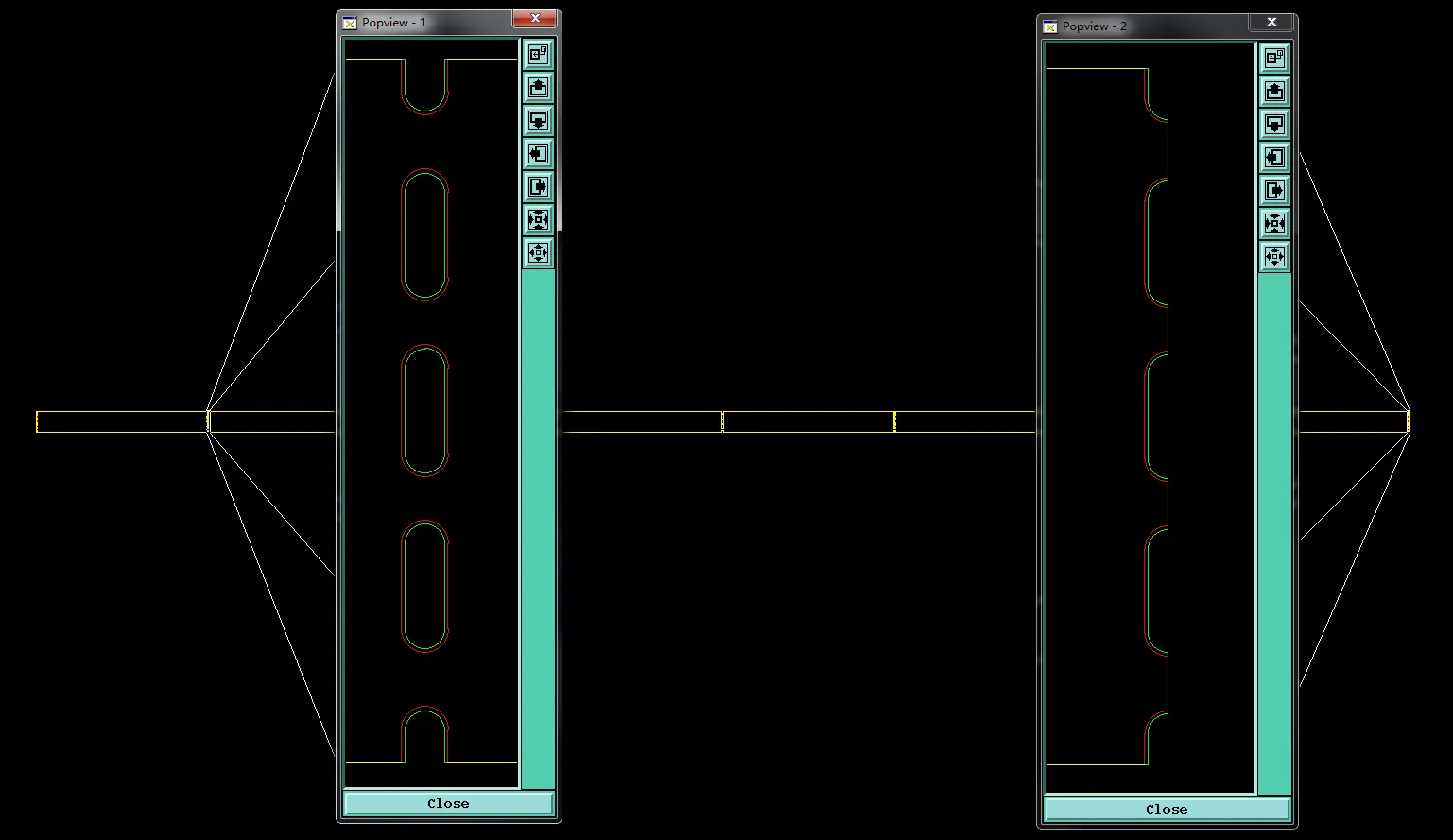
Figure 1: customer designed slots at 1.0mm width
We noticed this during the mechanical routing review. Our engineer recommended the adjustment because proceeding with 1.0mm slots could cause rough edges, dimensional inaccuracy, or even scrap boards. If ignored, the slots might have irregular shapes or cause delamination around the cut areas due to excessive mechanical stress on the aluminum.
Aluminum's rigidity makes fine milling particularly challenging. The customer approved the 1.2mm slot width after reviewing our proposed production file.
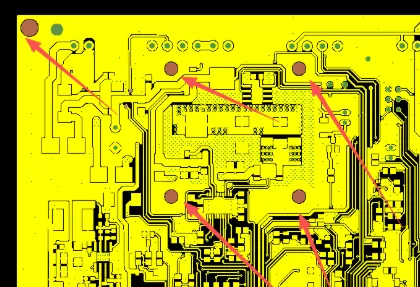
Copper to Edge Clearance and Exposed Copper Risk
Multiple copper features were positioned very close to the board outline. During V-cut and routing, this would likely result in exposed copper on the edges. We raised this issue and proposed selective copper removal to maintain proper clearance.
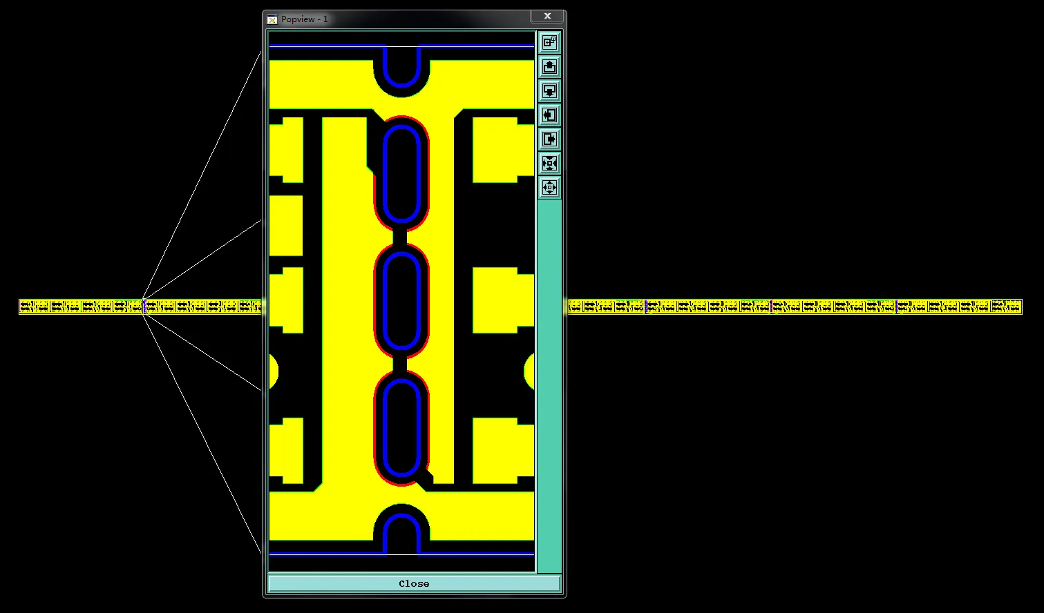
Figure 2: copper features were positioned very close to the board outline
Based on IPC-A-600 acceptability standards, exposed copper on aluminum PCB edges can lead to oxidation, reduced thermal performance, and potential short circuits in high voltage applications. If not addressed, this could cause cosmetic defects, poor OSP adhesion at the edges, or electrical failures during the required AC3000V testing.
Our CAM team identified these areas early and confirmed the copper pull-back with the customer to protect product reliability.
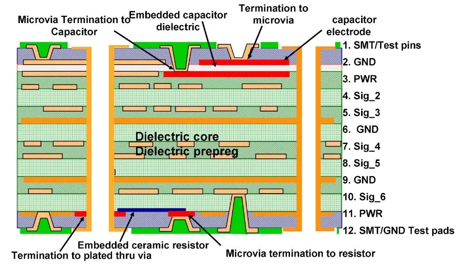
Dielectric Thickness and Base Material Substitution
The design specified a particular dielectric thickness that our standard aluminum material could not achieve. Additionally, we did not have the exact 72um base material in stock and proposed using either 50um or 100um alternatives.
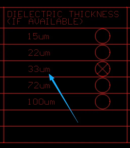
Figure 3: a particular dielectric thickness that our standard aluminum material could not achieve
After reviewing the stackup, we found these constraints conflicted with available production materials. Proceeding without confirmation risked inconsistent thermal conductivity and mechanical strength. The customer confirmed we could proceed with available material after evaluation.
Process Edge Modifications and Silkscreen Adjustments
To prevent deformation and scratching during handling, we proposed flattening the process edges and adding 1.0mm chamfers on all four corners. We also enlarged small characters on the silkscreen layer and accepted minor frame incompleteness to avoid ink on pads.
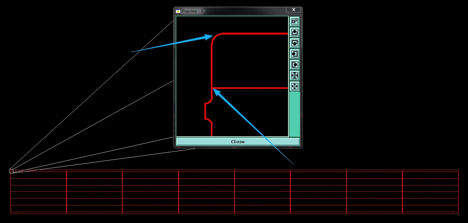
Figure 4: flattening the process edges and adding 1.0mm chamfers on all four corners
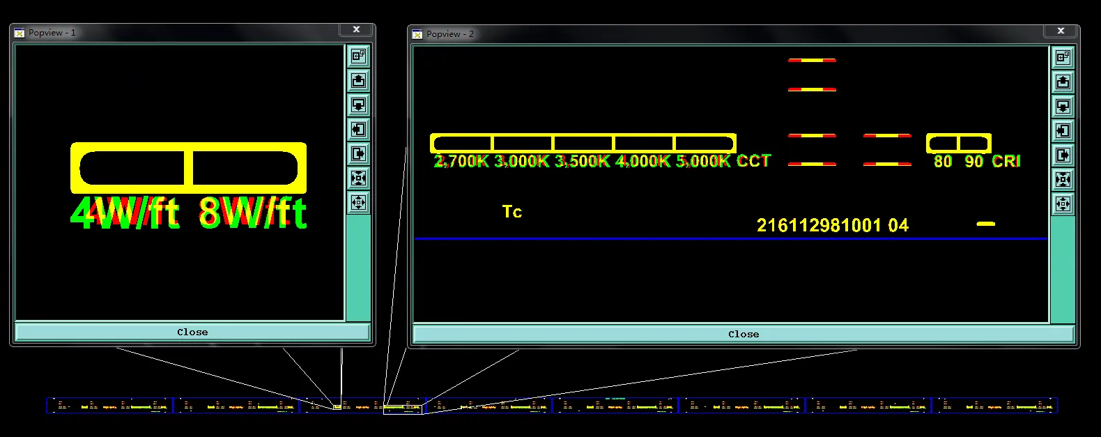
Figure 5: enlarged small characters on the silkscreen layer
These are standard practices for aluminum panels but require customer approval. We also confirmed using our standard solder mask ink and ignoring hole copper requirements since these were non-plated holes on a single-layer board.
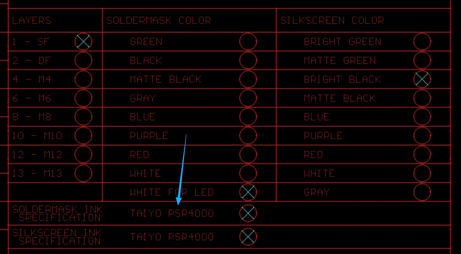
Figure 6: using our standard solder mask ink
Manufacturing Risks and DFM Insights
Aluminum PCBs commonly trigger EQs around mechanical processing limits and material availability. Designers often specify slot widths or dielectric thicknesses that exceed practical manufacturing capabilities for aluminum substrates. Edge copper proximity is another frequent issue that can compromise high-voltage reliability.
If these issues are ignored, results can include tool damage, dimensional out-of-tolerance boards, exposed copper oxidation, inconsistent thermal performance, and test failures. In one similar project, unadjusted narrow slots led to significant yield loss and production delays.
How the Engineering Team Resolved the Issues
Our engineering team prepared detailed markup files showing all proposed changes. For the slot width, we provided before-and-after comparisons and received approval to use 1.2mm. Edge copper was adjusted selectively to prevent exposure while preserving functionality.
We noticed the material thickness constraint early and suggested suitable alternatives. All other adjustments, including process edge chamfering and silkscreen optimization, were documented and confirmed. This collaborative approach reduced risk and streamlined production.
Final Manufacturing Outcome
All engineering questions were resolved with customer approval. Production files were updated with enlarged slots, adjusted edge clearances, approved material substitutions, and optimized process edges. The order was successfully released for fabrication.
Key Takeaways for PCB Designers
- Consult your fabricator's aluminum slot milling capability chart before finalizing narrow slot dimensions.
- Maintain adequate copper-to-edge clearance on aluminum PCBs to prevent exposure after routing or V-cut.
- Specify realistic dielectric thickness requirements based on standard aluminum material offerings.
- Account for material availability and allow reasonable substitutions for base thickness when necessary.
- Design process edges with chamfers or flats for better handling of aluminum panels.
- Consider silkscreen character size limitations early to avoid excessive enlargement or legibility issues.
- Clearly define non-plated hole requirements and surface finish expectations for single-layer aluminum designs.
FAQ
Q1: Why can't aluminum PCBs always achieve very narrow milled slots?
A1: Aluminum is much harder than FR-4, making fine milling prone to tool breakage and dimensional instability. Minimum reliable slot width is usually higher than on standard materials.
Q2: What happens if copper is too close to the edge on aluminum boards?
A2: Routing or V-cut can expose copper, leading to oxidation, reduced insulation, and potential failure in high voltage testing. Selective copper removal is often necessary.
Q3: Why do factories sometimes substitute aluminum base material thickness?
A3: Specific thicknesses may not be in stock. As long as thermal and mechanical performance remains acceptable, approved substitutions prevent production delays.
Q4: Should designers add process edge chamfers on aluminum PCBs?
A4: Yes. Chamfers reduce sharp edges that can cause scratching or deformation during handling and panel separation.
Q5: How important is edge copper clearance on OSP finished aluminum boards?
A5: Very important. Exposed copper oxidizes quickly and can compromise both appearance and electrical isolation, especially under high voltage stress.