OSP Aluminum PCB Production Record #ALU-20260120-012

| Parameter | Value | Parameter | Value |
|---|---|---|---|
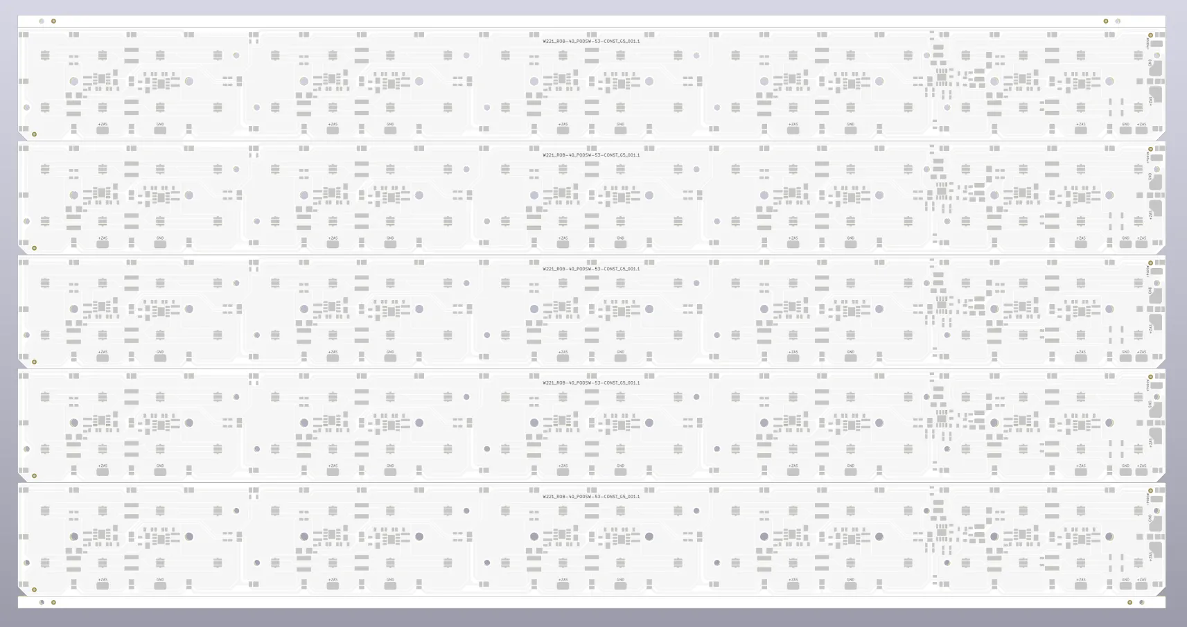
| PCB Type | Aluminum PCB | Quantity | 5 pcs |
| Layers | 1 Layers | Board Type | Panel PCB |
| Dimensions | 118.01 x 1193.8 mm | Copper Weight | 1oz |
| Thickness | 1 mm | Min Track / Spacing | 10/10mil |
| Surface Finish | OSP | Min Hole Size | 1.5mm↑ |
| Solder Mask | White | Silkscreen | Black |
| Thermal Conductivity | 3.0W | Voltage Withstand | AC3000V |
This single-layer aluminum PCB (118.01 × 1193.8 mm, 1.0 mm finished thickness, AL-01-B30L material with 3.0 W/m·K thermal conductivity) was produced in a 1×6 panel arrangement for a total of 30 pieces. The board used 1 oz copper, 10 mil minimum line/space, 1.5 mm minimum hole size, white solder mask on top with no bottom mask, black legend, and OSP surface finish. Production involved 100% AOI inspection, V-scoring, mechanical forming, and full high-voltage testing at AC3000V. The long, narrow form factor required careful handling during processing to maintain flatness.
DFM review addressed multiple aluminum-specific challenges. Process edges were chamfered at 1.0 mm and leveled to prevent deformation and scratching of adjacent boards. Edge copper features positioned too close to the outline were trimmed to avoid exposure after routing. Slot width was increased from the designed 1.0 mm to 1.2 mm due to the hardness of the aluminum substrate limiting smaller routing capability. Solder mask openings were enlarged by 0.05 mm on pads to prevent ink coverage, and small characters were scaled with acceptance of partial framing. Dielectric thickness requirements were waived as unachievable, and available core thickness (50 µm or 100 µm) was used in place of the specified 72 µm. Non-plated holes were processed without copper deposition as appropriate for single-layer construction. aluminum substrate machining limits and edge clearance were managed through these adjustments.
All engineering questions were confirmed with the customer before production release. The order was completed within the 10-day delivery window. Final quality documentation and electrical testing confirmed full compliance with the adjusted parameters.
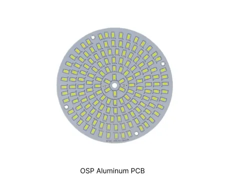
Aluminum core boards finished with OSP deliver cost-effective thermal performance and flat coplanarity for high-power SMT assembly.
Discover real factory insights on common engineering queries for HASL Aluminum PCB and OSP Aluminum PCB. As a senior PCB manufacturing engineer, I explain material-specific DFM challenges, surface finish conflicts with aluminum substrates, thermal management issues, and practical solutions to reduce EQs and improve production yield
| Order ID | PCB Type | Layers | Dimensions | Solder Mask | Surface Finish | Quantity | Action |
|---|---|---|---|---|---|---|---|
| ALU-20260511-016 | Aluminum PCB | 2 | 91 x 70 | Green | ENIG (Immersion Gold) | 10 | View detail |
| ALU-20260411-047 | Aluminum PCB | 2 | 102 x 227 | White | ENIG (Immersion Gold) | 10 | View detail |
| ALU-20260411-037 | Aluminum PCB | 2 | 105 x 59.5 | Black | ENIG (Immersion Gold) | 20 | View detail |


