2 Layer Aluminum PCB Production Record #ALU-20260511-016
| Parameter | Value | Parameter | Value |
|---|---|---|---|
| PCB Type | Aluminum PCB | Quantity | 10 pcs |
| Layers | 2 Layers | Board Type | Single PCB |
| Dimensions | 91 x 70 mm | Copper Weight | 3oz |
| Thickness | 2 mm | Min Track / Spacing | 10/10mil |
| Surface Finish | ENIG (Immersion Gold) | Min Hole Size | 0.2mm |
| Solder Mask | Green | Silkscreen | White |
| Thermal Conductivity | 3.0W | Voltage Withstand | AC2500V |
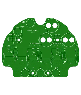
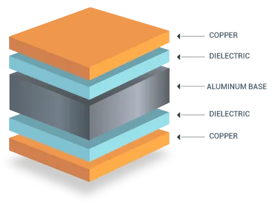
This 2-layer aluminum base PCB (91 × 70 mm, 2.0 mm finished thickness, LJ-C-AL3xxL material with 3.0 W/m·K thermal conductivity) was produced as single-unit panels for a quantity of 10 pieces. The board used 3 oz copper on the top layer, green solder mask, white legend, and ENIG surface finish. Production included 100% AOI inspection, resin plugging for specified vias, mechanical forming, and high-voltage testing considerations. The thick copper and aluminum substrate required specific process adaptations for reliable fabrication.
DFM review focused on material and thickness challenges inherent to 3 oz copper on aluminum. Copper features were trimmed by 0.3 mm on one side to prevent lifting and shorting during drilling. Dielectric thickness was adjusted from the initial 50 µm specification, as the thin insulation risked delamination with heavy copper; the revised stackup was confirmed with the customer. Solder mask application used two passes (initial transparent followed by standard green) to achieve coverage over the high copper profile. Large 3.2 mm and 6.0 mm holes were processed as NPTH due to aluminum substrate limitations. Character printing on thick copper accepted some fuzziness, with factory markings and production cycle added per request.
All engineering questions were confirmed before production release. The order completed within the 22-day delivery window. Final quality documentation and testing verified compliance with the adjusted parameters and controlled processes for this aluminum PCB build.
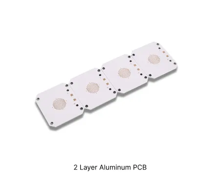
These PCBs feature two copper layers on an aluminum substrate with thin dielectric for thermal transfer. They support higher circuit density than single layer designs while maintaining superior heat dissipation.
Explore common engineering queries in 2 layer aluminum PCB manufacturing, including CTE mismatch, thermal via design, dielectric bonding, and solder mask registration issues. Learn practical DFM solutions to reduce warpage, improve thermal performance, and increase production yield.
| Order ID | PCB Type | Layers | Dimensions | Solder Mask | Surface Finish | Quantity | Action |
|---|---|---|---|---|---|---|---|
| ALU-20260120-012 | Aluminum PCB | 1 | 118.01 x 1193.8 | White | OSP | 5 | View detail |


