A solder paste aperture and a solder mask opening that do not match is a two-file conflict in one package. It is not a cue to make the layers identical, and extra flashes on the solder paste layer are not, by themselves, a request to copy that geometry onto solder mask.
This article stays on that conflict: what the released solder paste layer and solder mask layer show at the same site, what a paste-versus-mask overlay can and cannot prove, why the four mismatch classes are not one edit, and how the EQ is written so the reply can choose openings on the bare board without merging stencil data into resist. Paste volume, stencil thickness, and solder-mask dam capability are outside the scope.
| What arrives in the EQ | What the two files show | What is still open |
|---|---|---|
| Extra flashes on the solder paste layer — copy them onto solder mask? | Paste aperture present; solder mask still closed over that copper | Whether that copper is exposed on the finished board |
| Solder paste layer and solder mask layer do not match; which file to follow? | Same site tagged paste-only, mask-only, both present but different, or paste on no copper | Which sites are fabrication, which are stencil-only, which are leftover plot |
| Paste over a covered SMT land, test point, or via | Paste plotted; resist closed | Open the land, leave it covered, or treat paste as unused CAD output |
| Several paste flashes inside one solder mask opening | Window-pane or reduced paste on a land that already has an opening | Leave the difference on the stencil, or change the opening only if the reply names that change |
Two Files in One Package, Two Different Maps
The package already contains both files. One is the solder mask Gerber. The other is the solder paste Gerber. In a viewer they look like two maps of flashes on the same lands.
At one site the paste aperture is there and the solder mask opening is not. At the next site the opening is there and paste is empty. On a thermal land one opening covers the copper while several smaller paste apertures sit inside it. That site list is the review problem.
CAD plots both layers because the job contains both layers. Solder mask is fabrication data: openings in resist on the finished board. Solder paste is assembly data: stencil apertures if that file is used to cut a foil. File names and the layer list identify which is which. In that list only, GTS/GBS are solder mask and GTP/GBP are solder paste. CAD may still label the paste file "paste mask." That name does not change the role.
SMT lands often look similar on both files. That similarity is why someone asks CAM to make them the same. A fabrication note that never mentions the solder paste layer does not authorize a mask edit. An assembly note that never mentions solder mask does not authorize a stencil rewrite during fab review. Build the mismatch list by site before proposing an edit.
| Released object | Role in the package | What a flash on that layer means |
|---|---|---|
| Solder mask layer | Fabrication | Resist is open; copper at that site can be soldered, probed, or left as an exposed land |
| Solder paste layer | Assembly / stencil | Aperture in the foil if this file is used to cut a stencil |
| Fabrication note | Board construction | Can order openings, coverage, or finish. Does not rewrite paste by silence |
| Assembly note / centroid | Stuffing and print | Can mark no-stuff, fiducials, or stencil intent. Does not rewrite mask by silence |
What Paste-Versus-Mask Overlay Can Show
Overlay measures geometry. It does not assign ownership of the site.
Paste against solder mask produces four readable states: paste only, mask only, both present and different, both present and aligned enough to leave alone. Those sites against copper show whether a land, a via land, plane copper, or no copper sits under the mismatch. Those sites against drill show whether a via is involved.
A land that already has both an opening and an aperture, but a different shape or count, stays on a separate list from a site missing one file entirely. Side matters. A cluster of paste flashes on one thermal land is not the same finding as one extra paste flash on a via.
| Overlay | What it can show | What it cannot show |
|---|---|---|
| Paste vs solder mask | Paste-only, mask-only, both different, both aligned | Which file is the fabrication instruction |
| Mismatch sites vs copper | Land, via land, plane, or no copper under the flash | Whether that copper was meant to stay covered or become a solderable land |
| Mismatch sites vs drill | Via involved or not | Tent, plug, fill, or cap. Drill presence is not stencil intent |
Tag each site paste-no-mask, mask-no-paste, both-different, or no-copper. Record the side and whether paste is one flash or a cluster.
What the Overlay Does Not Measure
Overlay does not show whether the solder paste layer is a fabrication instruction. Some packages plot paste because the CAD job always plots it. That file may never be the production stencil.
It does not show whether a land was meant to stay solder-mask-defined, NSMD, or covered. A larger opening than the paste aperture is common on SMT lands. A smaller paste aperture than the opening is also common. Neither reading proves the other file is wrong.
It does not show stencil process. Volume, gasketing, and foil thickness belong to assembly after the board exists.
When reviewing PCB solder mask and via design issues, if the fabrication notes, assembly notes, and layer list contain no instruction assigning the paste file or requiring the two files to match, the mismatch list should remain an EQ. It is not an edit list.
Paste Aperture, No Solder Mask Opening
This is the class that gets read as "copy paste into mask."
Sites that show up here: an SMT land with paste and no opening; a test point opened only in paste; a via land or via-in-pad site with paste over covered copper; an unused or no-stuff land still plotted on paste. PTH and component-hole lands can appear in paste by CAD habit. That is not an SMT paste site.
If solder mask stays closed, the finished land is resist-covered. A later stencil can print paste onto solder mask, with no wettable copper under it. If an opening is added without confirmation, copper that was left covered becomes solderable, and a covered via can take solder into the barrel.
Fabrication does not apply solder paste. The live question is whether that copper is exposed on the finished bare board. Copper present, a net / pin / test-point attribute if the package carries it, and a drill hit are the checks. An assembly drawing or centroid, if present, separates stuffed from no-stuff.
If an opening is later agreed, the usable wording is "open solder mask over this land," not "draw the paste flash on the solder mask layer." The paste shape is stencil data. The opening follows the land unless the customer signs the paste shape as the opening artwork.
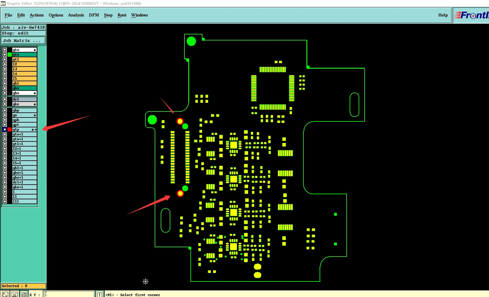
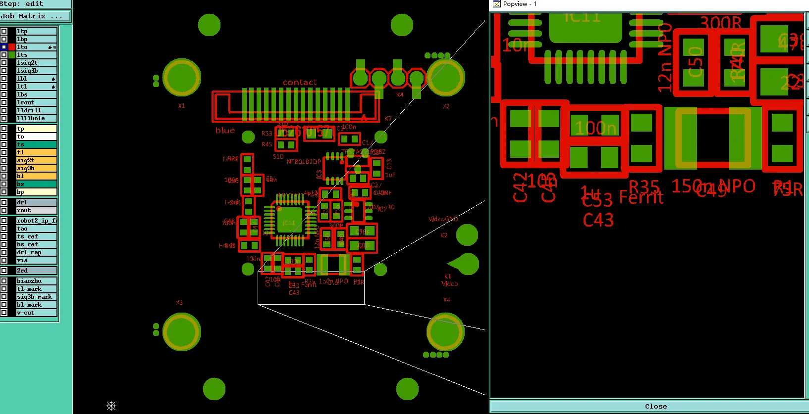
There is more openings in solder paste layer.
Solder Mask Opening, No Paste Aperture
Resist is open, but paste is not. The bare board will expose copper that this stencil file does not print.
Sites that commonly appear in this category include PTH and component-hole lands opened for soldering or probing but intentionally excluded from paste; fiducials opened so the camera can detect the metal while remaining paste-free; open vias or test points intended for probing or wave soldering rather than stencil printing; and SMT lands where paste is missing because the library disabled it or the plot omitted it.
An opening without paste is often correct fabrication. Closing the solder mask opening simply to match an empty paste layer is therefore the wrong default. The site becomes an EQ when it is an SMT land expected to receive paste. In that case, the missing data is stencil information, not solder mask.
If the paste file is included in the package only as CAD output, flag missing paste on SMT lands for assembly review rather than inventing an aperture to “complete” every opening. Separate PTH, fiducials, open vias, and SMT lands before writing the question. As part of a careful PCB DFM review, ask whether the empty paste site is an SMT omission or an intentionally paste-free location.
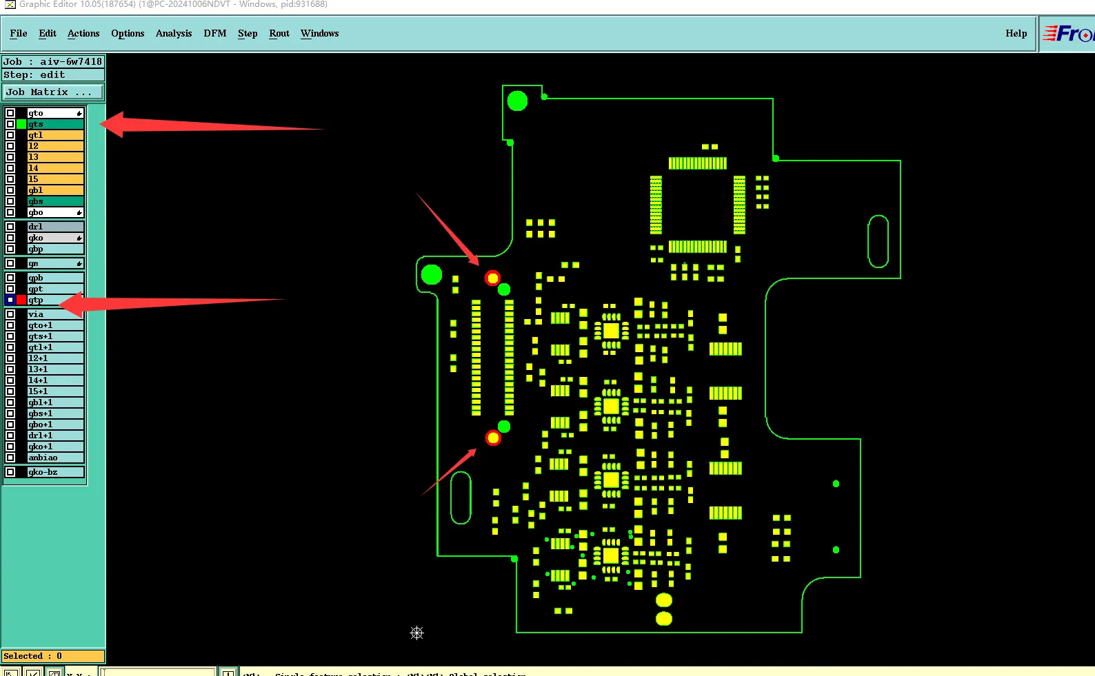
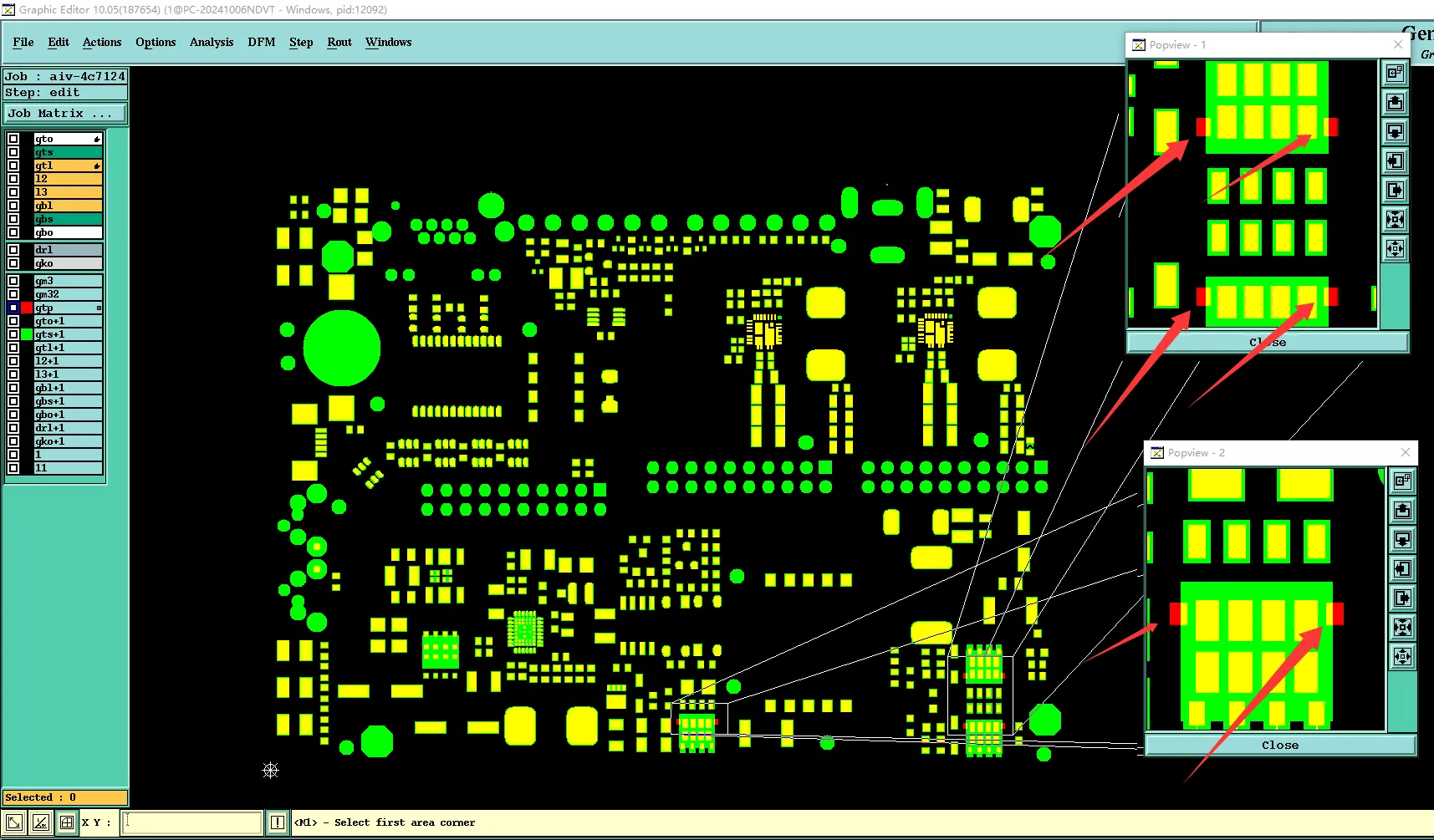
At the Mark point opening indicated by the arrow, the solder paste layer and the solder mask layer are inconsistent.
Both Present, Size or Count Does Not Agree
Difference checks treat any extra flash as a mismatch. Extra openings on the solder paste layer are not one case. What sits under the extra aperture decides the EQ.
When the paste layer contains more apertures than the solder mask layer, and those additional sites fall on lands, the factory may propose copying the paste geometry onto the solder mask layer so the finished board exposes the corresponding copper. However, that proposal should remain an EQ until the customer's reply identifies the specific lands. The practical resolution is then to create a solder mask opening over those lands. Using the paste flash directly as the opening artwork is acceptable only when the customer confirms and accepts that geometry.
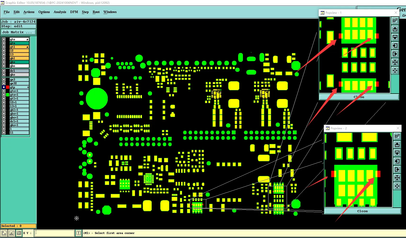
there is extra opening on paste layer
When the extra paste flashes are actually trace windows—apertures drawn over routing rather than over a land—they belong on a different mismatch list. Opening the solder mask in those locations would expose the underlying traces. In this type of PCB DFM production review, the usual written question is whether the board should follow the released solder mask data. The usual resolution is yes: keep the original solder mask and remove those trace apertures from the solder paste layer as well, so a later stencil does not print onto covered copper or laminate.
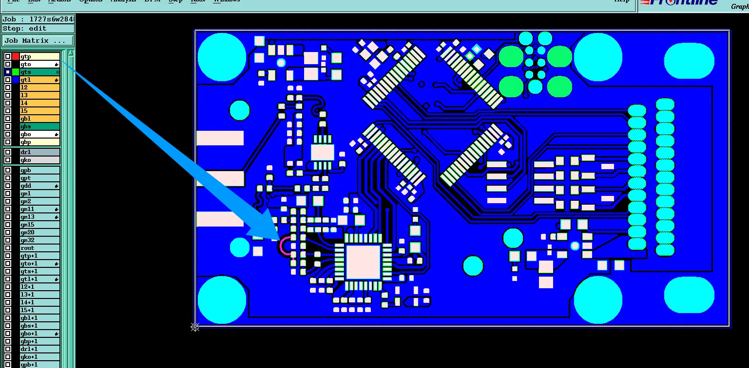
There is an extra figure on the top paste layer.
A land that already has both a solder mask opening and a paste aperture, but a different shape or count, stays off those two lists.
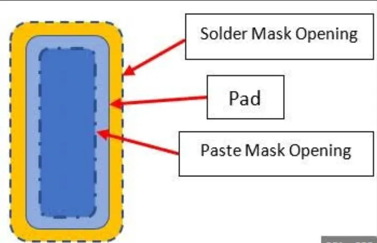
One solder mask opening over a thermal land, with several smaller window-pane apertures on paste, is a normal pair. The bars between those paste apertures are not solder mask dams. Paste pulled in from the land edge, with the opening at or beyond that edge, is also a normal SMT pair. Offset between aperture and opening is a registration or library note. It is not proof that one file should replace the other.
Copying still changes the board or the stencil when the site is the wrong class:
- Window-pane paste copied into solder mask leaves resist slivers on a land released as one opening.
- A reduced paste aperture used as the solder mask opening shrinks exposure and can turn an NSMD-looking land into a smaller, solder-mask-defined land with no one choosing that.
- The solder mask opening copied onto paste dumps full-opening volume onto a thermal land or fine-pitch land the paste file had already reduced or split.
- A trace window on paste copied onto solder mask exposes routing the released mask had left covered.
If a single solder mask opening already covers the land, treat the site as a stencil-only shape difference unless a note orders the files to match. If the opening is missing and only pane flashes exist on a land, that site belongs with extra paste over a land, not here. If the extra flash sits on a trace and not on a land, it belongs with the trace-window list: released solder mask stays, those paste apertures come off.
Make the Two Layers the Same File?
Paste geometry answers where solder paste is printed. Solder mask geometry answers where copper is exposed on the finished board. Those answers are allowed to differ.
Paste used as the mask source imports window-pane bars, reductions, and leftover flashes into resist. Mask used as the paste source puts paste on PTH lands, fiducials, open vias, and full thermal lands the paste file had already split or emptied.
A note that says "make them match" is still a customer instruction. Restate the direction: which sites gain solder mask openings, which sites gain or lose paste apertures, and that paste shapes are not default opening artwork. The usual fab close leaves the solder paste layer alone. Assembly owns stencil data unless the customer also revises it.
Do not run paste UNION mask or mask UNION paste as the working file for either layer. If an edit is needed, list the sites and the layer that will change.
| Close path | What stays | What changes | When it fits |
|---|---|---|---|
| A — keep both released files | Solder mask and solder paste as plotted | Nothing on the board artwork | Shape-only differences, window-pane, reduced paste, fiducial paste off, PTH mask open / paste off, leftover paste with no copper, covered vias left covered |
| B — change solder mask only | Paste left as assembly data | Named lands or test points opened or closed on solder mask | A site is named as exposed or covered on the bare board. Openings follow the land, not the paste flash, unless the customer signs the paste shape |
| C — mixed list | Some sites Path A, some Path B | Mask only where the reply names a fab change; paste only if stencil data is in scope | SMT lands missing paste called out for assembly rather than filled from mask |
What Has to Be True Before This EQ Can Close
The open decision is which mismatches are fabrication, which are stencil-only, and which are file noise.
Path A keeps both released files. Path B changes solder mask only. Path C is a mixed list, and paste changes only if the customer puts the stencil file in scope.
After the reply, re-overlay solder mask versus copper at the listed sites. Confirm paste was not merged into mask, and mask was not merged into paste. Update the solder mask Gerber only if Path B or C calls for it. Leave solder paste as assembly data unless the reply also revises stencil intent. No silent "match the two layers" compile.
How the Finding Is Written So the Reply Can Be Used
Attach the four-class split: paste-no-mask; mask-no-paste; both-different; no-copper. One example screenshot per class, plus a site list.
One fabrication question: which sites change on the solder mask layer of the bare board? One assembly question only if the paste file is in scope for stencil cut: which paste apertures stay, drop, or get added?
Skip "should the two files be identical?" Add a line that window-pane apertures are not copied into solder mask unless the reply says to.
What to Check in the Files Before Release
Overlay solder paste versus solder mask versus copper versus drill. Walk mismatches as a list, not as a layer merge.
An SMT land intended to solder still needs a solder mask opening. Paste on that land is a stencil choice, not proof of the opening. Covered vias, no-stuff lands, and test points meant to stay covered should not rely on "delete from paste later." If paste still shows them, say so in the assembly note.
Thermal land: one solder mask opening unless the land is truly split; window-pane stays on paste. Fiducial: solder mask opening on the copper mark; paste usually off. PTH and component hole: solder mask opening as required for that hole; paste usually off.
If paste is included so the assembler can cut a stencil, name it that way in the layer list. An opening that is supposed to exist on the finished board lives in the solder mask layer. The solder paste layer cannot carry that fabrication intent by itself.
FAQ
Q1: Do extra solder paste apertures need to be copied onto solder mask?
A1: Only if the reply names those sites as copper to expose on the bare board. Carry the need for an opening, not the paste flash, unless the customer signs the paste shape as the opening.
Q2: The two layers do not match. Which file do we follow?
A2: Each file for its job. Solder mask for resist openings. Solder paste for stencil apertures if that file is the stencil source. A mismatch list is not a license to pick one Boolean master.
Q3: Paste is larger than, smaller than, or offset from the solder mask opening. Is that a defect?
A3: Not by itself. Reduced paste inside a larger opening is common on SMT lands. Offset is a library or registration note. It becomes a fab EQ if the opening itself is wrong for the land.
Q4: A thermal land has one solder mask opening and several paste flashes. Should mask be split to match?
A4: No. That is a window-pane aperture on the stencil. Split mask only if the land itself is released as separate copper.
Q5: A fiducial is open in solder mask and empty in paste. Do we add paste?
A5: Usually no. The mark needs exposed copper for the camera. Paste on a fiducial is the exception.
Q6: Mask is open on an SMT land and paste is missing. Do we close the opening?
A6: No. If that land is expected to take solder, the missing object is stencil data. Flag it for assembly.