










A 4-layer FR-4 board measuring 233 mm × 179 mm entered CAM review as a customer-panelized 2 × 2 array with 8 mm process edges on all sides. The order specified TG130 material, 1.6 mm thickness, 0.5 oz inner / 1 oz outer copper, green solder mask on both sides, white silkscreen, immersion gold finish, aluminum-plugged vias, V-cut depanelization, and 100 % flying-probe testing. Quantity was 20 pieces across five sets. Minimum hole size was 0.2 mm and minimum track/space 6 mil. During data verification the solder-mask openings did not align cleanly with the SMT paste layer or the underlying copper pads and traces. In several locations the mask openings extended beyond the intended pads and exposed adjacent traces, creating a clear risk of solder wicking. The investigation therefore focused on establishing a manufacturable solder-mask opening design before the panel could be released for plating and mask application.
Intended SMT Pad Definition and Mask Clearance
The board ( #FR4-20260105-042 ) designer's apparent objective was a conventional SMT assembly panel in which solder-mask openings would expose only the copper pads while protecting neighboring traces. The paste layer defined the intended solderable areas, and the copper layers contained the corresponding pads plus connecting traces. On a 4-layer board with immersion gold and aluminum-plugged vias the surface must remain free of unintended exposed copper so that solder stays confined to the pads during reflow. The fabrication data, however, showed mask openings that were larger than the paste features and that overlapped trace segments. Without correction those openings would allow solder to wet the traces, producing bridging, reduced insulation resistance, or cosmetic defects that fail IPC-A-600 Class 2 criteria.
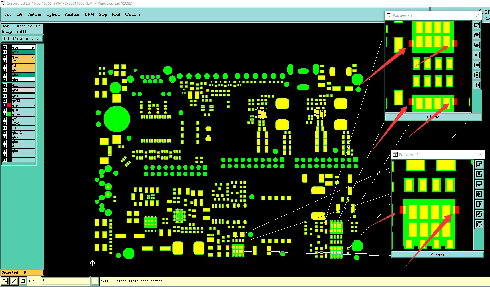
Figure 1: there is extra opening on paste layer
Paste Layer Versus Solder Mask Opening Mismatch
Our CAM engineer compared the SMT paste layer directly against the solder mask layer. In multiple regions the mask openings exceeded the paste apertures and extended over copper traces that carried pads. The traces themselves were continuous; once the mask was opened the copper would be fully wettable by solder. On an immersion-gold surface the gold finish further promotes solder flow, increasing the likelihood that solder would travel along the exposed trace segments during assembly. The factory's standard practice is to generate mask openings from the paste layer or from a controlled expansion of the copper pads; when the supplied mask data already contain oversized openings, the CAM system must either accept the risk or propose a corrective edit.
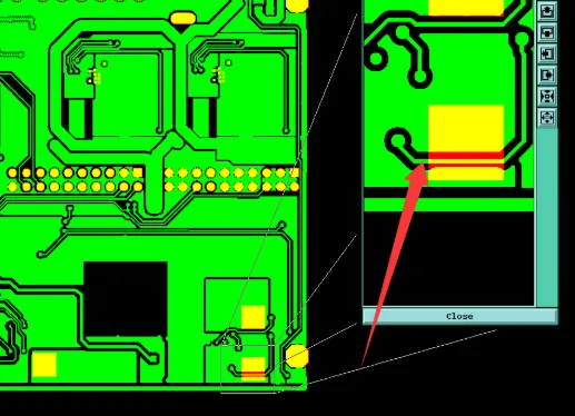
Figure 2: the solder mask opening may cause the traces open with tin
If the oversized openings had been left unchanged, two realistic manufacturing outcomes were expected. First, solder would wick along the exposed traces, creating solder bridges between adjacent nets or forming irregular fillets that fail visual and electrical inspection. Second, the unprotected trace segments would remain vulnerable to oxidation or handling damage before assembly, potentially elevating contact resistance. Either result would have reduced yield on a 20-piece panel and required costly rework or scrap.
| Layer Comparison | Observed Condition | Manufacturing Consequence | Proposed Correction |
|---|---|---|---|
| Paste vs Solder Mask | Mask openings larger than paste apertures | Excess copper exposed | Copy paste geometry to mask layer |
| Mask vs Trace Copper | Openings overlap continuous traces | Solder wicking along traces | Clear mask openings to cover traces |
| Pad Presence | Traces carry legitimate pads | Pads must remain exposed | Preserve pad openings while covering traces |
Primary Conflict: Uncontrolled Solder Mask Openings Over Traces
The dominant conflict was a data-to-data mismatch between the solder-mask layer and the combined paste and copper data, producing a manufacturing-interpretation problem. The supplied mask openings did not follow either a pad-defined or a paste-defined rule; instead they created irregular clearances that left trace segments exposed. On a board finished with immersion gold the exposed copper would accept solder readily, violating the design intent of confining solder to the SMT pads. Because the panel already carried aluminum-plugged vias and a defined V-cut array, any post-mask solder defects would be difficult to rework without damaging the gold finish or the plugged vias.
Design intent could not be confirmed from the files alone. The presence of pads on the traces indicated that those pads were meant to be solderable, yet the oversized mask openings simultaneously exposed the connecting lines. The factory therefore could not decide whether the designer intended non-solder-mask-defined pads with intentional trace exposure or whether the mask data simply contained an expansion error. Production release was blocked until a single, consistent mask geometry was agreed.
Supporting Observations on Panel and Via Features
Secondary findings reinforced the need for precise mask control. The 2 × 2 customer panel used V-cut separation with 8 mm process edges; any solder bridges that formed near the V-score lines would be difficult to inspect or correct after depanelization. Aluminum-plugged vias require a clean, planar surface for reliable plugging and subsequent gold plating; residual solder on nearby traces could interfere with that planarity. These observations did not generate independent primary holds, yet they confirmed that mask-related solder defects would propagate into later process steps and final yield.
Mask Geometry Correction and Customer Confirmation
The engineering proposal contained two complementary edits. First, the SMT paste geometry would be copied onto the solder-mask layer so that every intended pad received a controlled opening while excess clearance was removed. Second, where mask openings still overlapped continuous traces, the openings would be locally cleared (pulled back) so that the mask covered the trace segments and left only the pads exposed. The resulting mask would therefore be paste-defined for the SMT features and would protect all non-pad copper.
The reply also stated that the production file had already been prepared according to these suggestions. If the customer confirmed the files contained no other errors, the two mask corrections would be implemented; otherwise a further confirmation cycle would be required and the three-day lead time would be affected. Customer acceptance was received without additional changes. The solder-mask layer was regenerated from the paste data with local trace coverage, the remaining CAM checks were closed, and the panel was released for fabrication.
| Engineering Observation | Conflict Identified | Recommended Action | Final Status |
|---|---|---|---|
| Mask openings larger than paste apertures | Excess copper exposure | Copy paste layer to solder mask | Implemented |
| Openings overlap continuous traces | Solder-wicking risk | Clear mask to cover traces | Implemented |
| Pads present on affected traces | Pads must remain solderable | Preserve pad openings | Confirmed |
Design Lessons for Reliable Solder Mask Opening Control
- Generate solder-mask openings from the paste layer or from a controlled expansion of copper pads; never allow mask clearances to extend over continuous traces.
- On immersion-gold boards any exposed trace segment will accept solder readily; mask coverage of non-pad copper is essential to prevent wicking.
- When pads sit on traces, the mask must expose the pads while still covering the connecting line segments.
- Verify paste-to-mask alignment in CAM before release; oversized openings are a frequent source of post-assembly solder bridges.
- Aluminum-plugged vias and V-cut panels leave little margin for rework; mask-related solder defects are best eliminated at the data stage.
- If the supplied mask data already contain errors, request a single confirmation cycle that authorizes the corrective edit and avoids repeated file exchanges.
- Document the intended mask rule (pad-defined or paste-defined) in the fabrication notes so that CAM interpretation remains unambiguous.
FAQ
Q1: Why do oversized solder-mask openings cause solder wicking on traces?
A1: Once copper is exposed beyond the pad, molten solder flows along the trace during reflow, especially on immersion-gold surfaces that promote wetting.
Q2: How does copying the paste layer onto the solder-mask layer solve the problem?
A2: The paste apertures define the exact solderable areas. Using them as the mask openings guarantees that only the intended pads are exposed.
Q3: What happens if mask openings overlap continuous traces but pads must stay exposed?
A3: The openings are locally pulled back so the mask covers the trace segments while the pad areas remain clear, preserving solderability of the pads only.
Q4: Why is this issue more critical on boards with aluminum-plugged vias?
A4: Plugged vias require a planar surface for reliable filling and subsequent gold plating. Solder on adjacent traces can disrupt that planarity and create voids or uneven plating.
Q5: Can V-cut panels tolerate solder bridges near the score lines?
A5: No. After depanelization the bridges become permanent edge defects that are difficult to inspect or remove without damaging the board.
Q6: How should designers prevent solder-mask opening mismatches?
A6: Generate the mask layer from the paste data or from a controlled pad expansion, then verify that no trace copper remains exposed outside the intended pads.






