










A 12-layer FR4 board measuring 235.13 mm × 259.7 mm arrived for production with TG170 material, 2.0 mm finished thickness, 1 oz copper on all layers, red solder mask, white silkscreen, ENIG finish, resin-plugged vias, and controlled impedance. Quantity was ten pieces. The design included back drilling, impedance requirements, and customer-supplied panelization with router separation. From a DFM perspective, the combination of high layer count, back drilling, and impedance control immediately raised questions about manufacturing stability. Our engineering team reviewed the data against the fabrication notes and identified several issues that could affect yield and long-term reliability if left unresolved.
The primary concern was not whether the board could be built, but what risks would appear if production continued without clarification. Back drilling would leave visible dimples on the finished board. Certain holes that looked like plated through-holes were defined as non-plated. Many impedance traces listed in the notes could not be located in the Gerber data. Material substitution and incomplete silkscreen characters added further uncertainty. Each of these points required preventive action before the first panel entered the press.
Why This 12-Layer Design Needed Careful DFM Scrutiny
High-layer-count boards ( #FR4-20260731-064 ) with controlled impedance and back drilling carry inherent process sensitivity. The board used Shengyi S1000-2M material at TG170. Copper was balanced at 1 oz inner and outer. Surface finish was ENIG with 2 µin gold. Vias were specified for resin plugging. Impedance control and an impedance report were both required. Process edges were zero, and the customer handled panelization.
These parameters are manageable when the data is clean. In this case the data contained gaps. One ART layer mapped to inner layer 7 showed no content. Back-drill locations were present, yet the finished-board impact of those drills was not addressed. Hole attributes conflicted with the graphical appearance of the pads. Impedance notes listed traces that could not be found in the design files. From a manufacturing stability standpoint, any of these issues could produce scrap, electrical failure, or assembly problems if ignored.
Our CAM engineer therefore treated the review as a risk-prevention exercise rather than a simple data check. The goal was to surface every condition that could compromise yield or reliability before the board reached the press.
Critical Back Drilling and Hole Definition Risks Found
Three issues ranked highest by potential impact.
The first was back drilling. The design required back drilling on selected vias. After the back-drill operation the finished board would retain small dimples or recesses at those locations. These dimples are a normal result of removing the unused stub, yet they affect surface planarity. On a board that must accept components or connectors near the drill sites, the recesses can create uneven seating, solder voids, or cosmetic rejection. The fabrication notes did not state whether the dimples were acceptable or whether any secondary fill was required.
The second critical issue was hole-type mismatch. Graphical review showed two groups of holes that clearly appeared as plated through-holes. In the drill and attribute data, however, they were defined as non-plated through-holes (NPTH). If processed as NPTH, those holes would receive no copper plating. The result would be open circuits where electrical connection was intended, or mechanical weakness if the holes were meant to carry current or provide structural support. This conflict is a classic CAM red-flag because the visual intent and the digital attribute do not match.
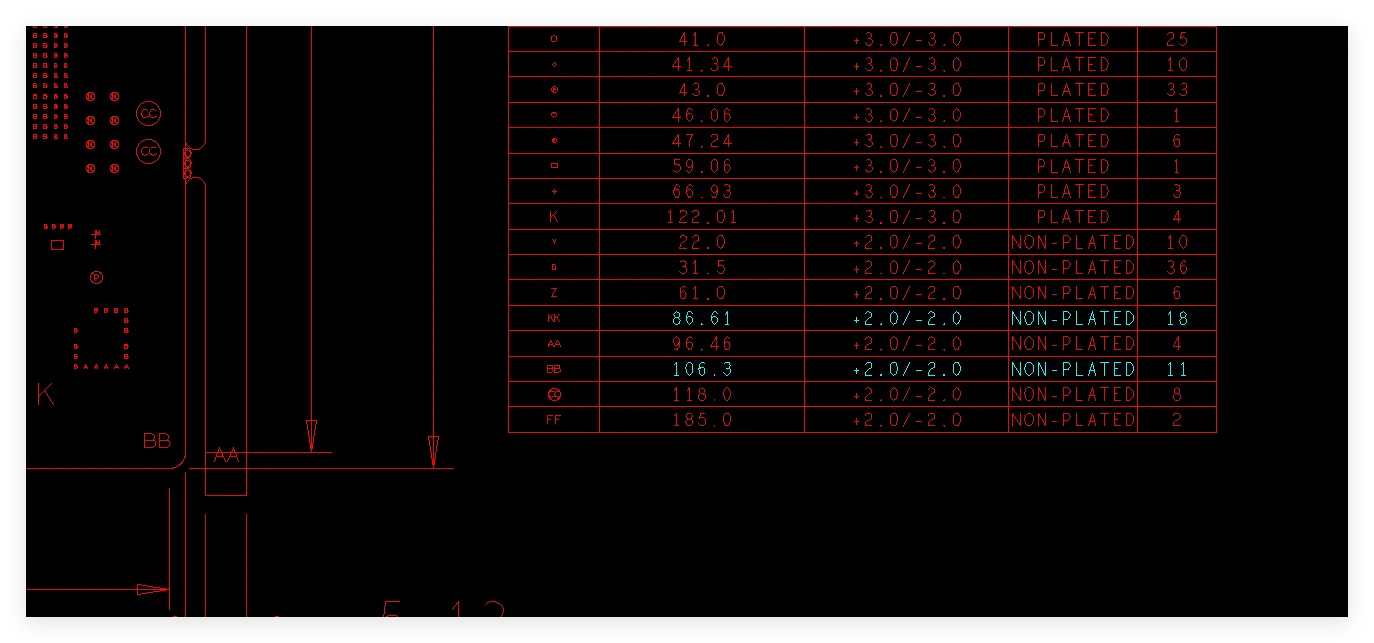
Figure 1: the two types of holes appear to be PTH holes but are currently defined as NPTH holes
The third major risk involved impedance control. The notes listed multiple controlled-impedance traces. When the Gerber and stack-up data were examined, many of those traces could not be located. Only the traces that could be positively identified would be controlled. On a 12-layer board with impedance requirements, missing or uncontrolled nets create signal-integrity uncertainty and raise the chance of electrical test failures or field performance problems.
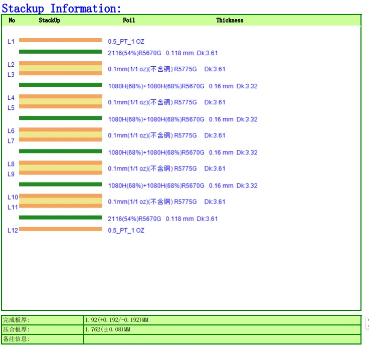
Figure 2: our impedance stack-up information
Secondary but still important items included the proposed material substitution (customer specified M-890K and EM-89BK; the factory planned to use equivalent Panasonic M6), incomplete silkscreen characters, missing content on the layer corresponding to L7, unclear serial-number and batch-code rules, and a question about QR-code printing. Each of these received attention, but the back-drill dimples, PTH/NPTH mismatch, and impedance gaps carried the highest risk of yield loss or reliability impact.
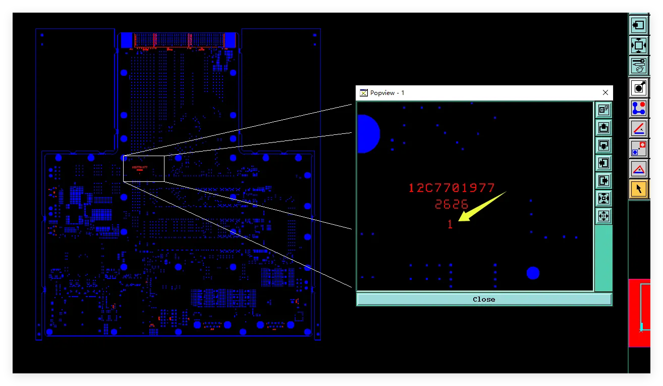
Figure 3: addition of the serial number
| Risk Area | Observed Condition | Severity |
|---|---|---|
| Back drilling | Dimples remain on finished board after stub removal | High – planarity & assembly |
| Hole attributes | Graphically PTH holes defined as NPTH | High – open circuit risk |
| Impedance control | Many listed traces not found in design files | High – signal integrity |
| Material | Specified M-890K/EM-89BK to be replaced by Panasonic M6 | Medium – performance match |
| Silkscreen | Some characters incomplete or broken | Medium – readability |
Table 1. Risk ranking used during the DFM review. Back drilling dimples, hole-type mismatch, and missing impedance traces were treated as the highest-priority items because each could directly affect yield or electrical performance.
How Back Drill Dimples and Hole Errors Could Affect Yield
If the back-drill dimples had been left unaddressed, the finished boards would have carried small recesses at every back-drilled location. These recesses reduce local planarity. During assembly, components or connectors placed over or near the dimples can sit unevenly, producing solder voids, insufficient joint strength, or mechanical stress on the solder joints. In high-reliability applications the same recesses can also trap flux or cleaning residue. IPC-A-600 treats surface irregularities that affect assembly as potential defects when they exceed local flatness expectations.
The PTH-versus-NPTH conflict carried an even more direct electrical risk. Processing a plated hole as non-plated removes the copper barrel. Any net that relied on that hole for continuity would become an open circuit. On a 12-layer board the open could remain undetected until flying-probe or functional test, at which point the entire panel or lot would be at risk of scrap. Even if the hole was only mechanical, the lack of plating reduces pull-out strength and can allow moisture ingress, both of which degrade long-term reliability under IPC-6012 criteria.
Missing impedance traces created a different but equally serious problem. The factory can only control the impedance of nets that can be positively identified and measured. Uncontrolled nets may fall outside the required tolerance. On a board that already requires an impedance report, the result is either a failed report or a board that passes electrical test yet fails in the system because of signal reflections or timing errors. Either outcome produces yield loss or field returns.
Material substitution added a further variable. Panasonic M6 is a known high-performance FR4 equivalent, yet dielectric constant, loss tangent, and resin system must still be confirmed against the original M-890K and EM-89BK specifications, especially for a TG170, impedance-controlled design. An unconfirmed substitution can shift impedance values or alter thermal-mechanical behavior enough to affect warpage or delamination risk.
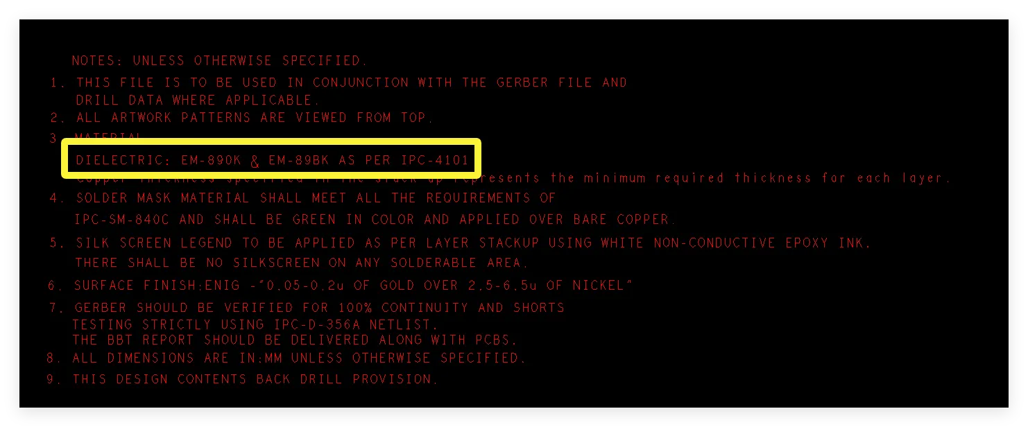
Figure 4: The requirement is for M-890K & EM-89BK materials
How Unresolved Back Drill Dimples Could Have Triggered Assembly Failures
The engineering discussion focused on concrete outcomes that would appear if the file had been released without clarification.
If back drilling proceeded without customer awareness of the dimples, the finished boards would reach assembly with unexpected surface recesses. Placement equipment or operators could struggle with coplanarity, leading to incomplete solder joints or rework. In the worst case, boards would be rejected at incoming inspection for surface finish or flatness issues, turning a ten-piece order into scrap.
If the PTH holes defined as NPTH had been processed as non-plated, the affected nets would show open circuits at electrical test. Because the holes looked plated in the graphics, the failure would appear as a mysterious open rather than an obvious design error. Debugging would consume time, and the lot could be delayed or rejected.
If impedance control had been limited only to the traces that could be found, some critical nets would leave the factory with uncontrolled impedance. The impedance report would be incomplete. Downstream system testing could then reveal signal integrity problems that were never caught at the PCB level, shifting the cost of failure from fabrication to the customer's assembly and field stages.
These scenarios are realistic manufacturing outcomes, not theoretical extremes. Each has been observed on similar high-layer-count, impedance-controlled programs when data conflicts were left unresolved.
Customer Confirmations That Fixed Dimples, PTH Attributes, and Impedance Gaps
Every Engineering Question was presented with clear evidence and a recommended path forward.
On back drilling, the team explained that dimples would remain on the finished board after stub removal. The customer confirmed that the dimples were acceptable for the intended application and that no secondary fill was required. This confirmation allowed production to proceed with the standard back-drill process while documenting the surface condition for the traveler and the quality report.
On the hole-type mismatch, the graphical evidence was shown alongside the attribute data. The customer confirmed that the holes in question were intended to be plated. CAM corrected the attributes from NPTH to PTH so that the holes would receive proper copper plating and solder-mask treatment consistent with their electrical function.
For impedance, the team listed every trace that could be positively identified and stated that only those nets would be controlled and reported. The customer accepted the limitation and confirmed that the unlocated traces did not require impedance control. The impedance report was therefore limited to the verified nets, avoiding false claims of control on non-existent features.
Material substitution was presented with the performance data for Panasonic M6 versus the original M-890K and EM-89BK specifications. The customer accepted the equivalent material. The stack-up was adjusted accordingly while preserving the required TG170 and impedance targets.
Incomplete silkscreen characters were enlarged or clarified where critical identification was needed. The missing content on the layer corresponding to L7 was confirmed as intentional (no circuitry required). Serial-number and batch-code rules, including position and QR-code requirements, were clarified so that marking could be applied consistently.
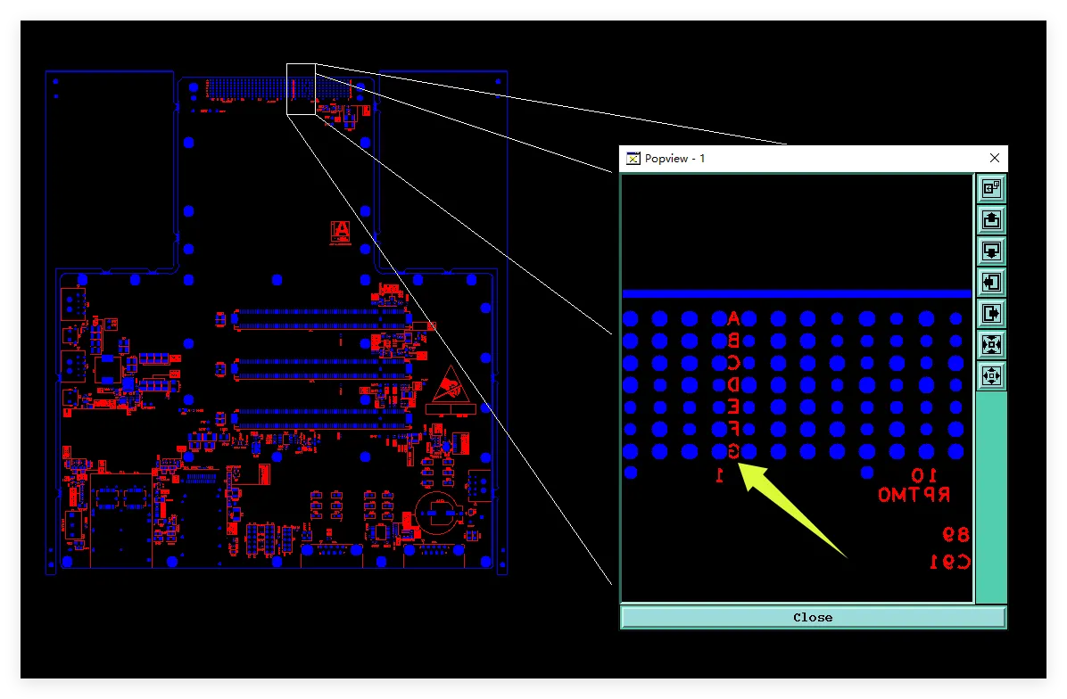
Figure 5: Some characters may appear incomplete
All confirmations were recorded, the files were updated, and the order was released. The sequence of clarifications removed the highest-risk conditions before any panel was pressed.
| Issue | DFM Recommendation | Customer Decision |
|---|---|---|
| Back drill dimples | Confirm acceptance of surface recesses or request fill | Dimples accepted as-is |
| PTH vs NPTH | Change attributes to PTH so holes receive plating | Confirmed as PTH – attributes corrected |
| Impedance traces | Control and report only identifiable nets | Accepted – only found traces controlled |
| Material | Use Panasonic M6 as performance equivalent | Accepted |
Table 2. Summary of preventive actions and customer decisions. Each change was driven by a concrete manufacturing risk rather than preference.
Why Early Back-Drilling Clarification Protected 12-Layer Board Reliability
This 12-layer order demonstrates that the most costly defects are often the ones that can be stopped at the engineering-question stage. Back-drill dimples, misdefined holes, and missing impedance nets were all visible in the data. None required exotic process capability to resolve. They required only clear communication and a willingness to adjust attributes or document limitations before fabrication began.
From a DFM standpoint, the value of the review is measured in avoided scrap, avoided electrical failures, and avoided assembly problems. A ten-piece lot that arrives with correctly plated holes, documented surface conditions, and controlled impedance on the nets that matter gives the customer usable boards rather than a troubleshooting exercise. The same disciplined approach scales directly to higher-volume programs where the cost of the same defects multiplies rapidly.
Designers and purchasing teams that engage early with manufacturability questions gain more than a clean file. They gain a more stable process window and a higher probability that the finished board will perform as intended over its service life. That is the practical outcome of treating every Engineering Question as a risk-prevention opportunity rather than a delay.
FAQ
Q1: Why do back-drilled holes leave dimples on the finished board?
A1: Back drilling removes the unused portion of a plated via to reduce stub length. The drill leaves a small recess or dimple at the surface where material was removed. These dimples are a normal process result. If components or connectors sit near the locations, the recesses can affect planarity and solder joint quality. Confirming acceptance or requesting a fill step prevents later assembly surprises.
Q2: What happens if a plated hole is processed as non-plated?
A2: The hole receives no copper barrel. Any electrical net that relied on that hole becomes an open circuit. Mechanical strength is also reduced, and moisture can enter the unplated barrel. On a multi-layer board the failure may not appear until electrical test or system assembly, at which point scrap or rework costs are already incurred. Correcting the attribute before plating eliminates the risk.
Q3: Why is it risky when impedance notes list traces that cannot be found in the Gerber files?
A3: The factory can only control and report impedance on nets that can be positively identified and measured. Unlocated traces remain uncontrolled. The resulting impedance report is incomplete, and the uncontrolled nets may fall outside tolerance. On a 12-layer impedance-controlled board this creates signal-integrity uncertainty that can appear as test failures or field performance issues.
Q4: Is material substitution from M-890K/EM-89BK to Panasonic M6 always safe?
A4: Panasonic M6 is a recognized high-performance FR4 equivalent, but dielectric constant, loss, and resin system must still be verified against the original specifications, especially for TG170 and controlled-impedance designs. An unconfirmed substitution can shift impedance values or alter thermal-mechanical behavior. Customer confirmation after data comparison keeps the risk low.
Q5: How can incomplete silkscreen characters affect a production lot?
A5: Broken or missing characters reduce readability of reference designators, polarity marks, or serial numbers. Inspection and assembly teams lose a primary visual reference, increasing the chance of orientation or identification errors. Enlarging or clarifying only the critical characters is usually sufficient to restore reliable identification without redesigning the entire legend.
Q6: Why should serial-number and batch-code rules be confirmed before production?
A6: Without clear rules for content, format, position, and optional QR-code printing, the marking applied by the factory may not match the customer's traceability system. Boards can then fail incoming inspection or create downstream tracking problems. A short confirmation of the exact marking requirements prevents these administrative and quality issues.






